67021-ultraviolet-led-multi-chip-module-based-on-ceramic-substrate.pdf - 第4页
Stresses are significa ntly lo wer than for the sold er attach a nd th us belo w t he ul timate tensile stresses of the substrate materials. D ue to lo wer Yo ung’s modulus of the adhesive – 1.2 GP a compared to 68 GP a …
UVA emitting indium-gallium-aluminum-nitride
LED-chips SL-V-U40AC by Semiled Inc. with a
center wavelength of 395 nm, a chip size of
1070×1070 µm² and a rated typical optical output
power of 210 mW to 250 mW are used. The initial
design was based on NS375C-3SAA LED-chips by
Nitride Semiconductor Co., Ltd. with a chip size of
600×600 µm² but was changed to the former due to
considerations of wavelength, optical output power
and availability. The Semiled chips are available
with a back metal gold layer usable for soldering
and adhesive bonding.
Electrical contacting of the front contact is con-
ducted by ultrasonic assisted wedge-wedge wire
bonding of Au and AlSi wires. Back-side contacts
are connected by the solder or the conductive adhe-
sive to the wiring structures on the substrate. Sub-
modules are mounted to a scalable and liquid-
cooled heat-sink by means of indium foil. The use
of indium allows for a proper thermal contact and
excellent cooling due to its high ductility and its
high thermal conductivity of 82 W/(m·K).
Thermo-mechanical and thermal simulations
Based on the design data and the NS375C-3SAA
LED-chips thermal and thermo-mechanical
analyses are conducted by finite elements si-
mulations (FE). Thermo-mechanical analysis is
used to evaluate the stresses to substrate, LED-
chips and joining material due to different
coefficients of thermal expansion. Thermal analysis
provides insight in the capability of the design and
material selection on efficient heat removal from
the chips. FE analysis is computed using ANSYS
11.0 SP1.
Targeted design goals are 80 mW optical output
power and 100 mW respectively. The LED-chips
achieve 80 mW optical at 200 mA, 4.5 V and about
9.5% efficiency resulting in a thermal load of
840 mW. 100 mW optical are attained at 350 mA,
5 V with less than 6% efficiency and a resulting
thermal load of 1650 mW. A ¼-model with sym-
metric boundary conditions is used for simulation.
Base temperature of the substrate is set to 0°C and a
natural convection with 10 W/(m²·K) is applied to
all outer surfaces. Table 1 shows relevant material
properties used for the simulations. Additionally
temperature dependency for Young’s modulus,
Poisson’s ratio and plasticity of the gold-tin solder
are modeled.
Modeling soldering using eutectic AuSn with a
solder layer of 10 µm is done. Solidification of the
solder alloy from solidus to room temperature leads
to a shrinking of about 5%. Resulting mechanical
stresses within the solder layer are near the yield
strength of the material indicating plastic defor-
mation of the solder. Maximum values of 320 MPa
for AlN and 337 MPa for Al
2
O
3
are calculated.
Stresses within the base materials are computed to
be 93 MPa for AlN and 95 MPa for Al
2
O
3
which is
significantly below the ultimate tensile stresses for
those materials.
Table 1: Material properties for simulation
model (sources: [21], [22], [23] and respective
data sheets,
(1)
┴
C-axis).
Property λ TCE E ρ
Unit W/K·m ppm/K GPa g/m³
Al
2
O
3
24 6.8 340 4.0
AlN 180 4.7 320 3.3
Sapphire 40 5.4
(1)
430 4.0
Au80Sn20 58 16 59 14.7
Adhesive 17 30 1.21 3.2
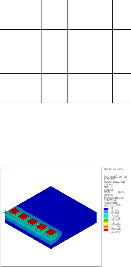
Thermal analysis is conducted to provide results of
temperature distribution and heat flux within the
sub-assemblies. For the design goal of 100 mW
optical output power per chip and a thermal load of
1.65 W chip temperatures are calculated to be 23 K
above substrate temperature for AlN and 40 K for
Al
2
O
3
using 10 µm AuSn solder layers (Figure 2
and Figure 3).
Figure 2: Temperature distribution within LED-
chips and AlN substrate (thickness 1 mm) for
eutectic AuSn solder (layer thickness 10 µm) and
1.65 W thermal load.
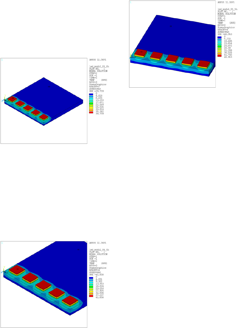
Calculations are repeated with respect to a con-
ductive silver-loaded thermoplastic/thermoset adhe-
sive with a thermal conductivity of 17 W/(m·K).
Assumed thicknesses of the adhesive layers are
10 µm and 30 µm respectively. Substrate material
is Al
2
O
3
with a thickness of 0.38 mm. Thermo-
mechanical strain is mainly influenced by the base
material and not the adhesive. Equivalent stresses
are 43 MPa for both adhesive layer thicknesses.
IMAPS/ACerS 8th International CICMT Conference and Exhibition (2012) | April 16-19, 2012 | Erfurt, Germany
000240
Downloaded from http://meridian.allenpress.com/imaps-conferences/article-pdf/2012/CICMT/000238/2360912/cicmt-2012-tp61.pdf by guest on 03 January 2023
Stresses are significantly lower than for the solder
attach and thus below the ultimate tensile stresses
of the substrate materials. Due to lower Young’s
modulus of the adhesive – 1.2 GPa compared to
68 GPa for AuSn – the inherent stresses within the
adhesive layers are significantly lower than within
the solder. The results show equivalent stresses
within the adhesive of 3.1 MPa for 10 µm layers
and 2.6 MPa for 30 µm layers, respectively.
Figure 3: Temperature distribution within LED-
chips and Al
2
O
3
substrate (thickness 0.38 mm)
for eutectic AuSn solder (layer thickness 10 µm)
and 1.65 W thermal load.
Thermal analysis for a thermal load of 1.65 W per
chip results in chip temperatures of 42 K above
substrate temperature for 10 µm layers and 47 K for
30 µm layers (see Figure 4 and Figure 5). These
calculations indicate that a proper cooling of the
chips could be achieved using thermally conductive
adhesives. Thicker adhesive layers increase chip
temperature significantly. In the case of thin
bonding layers – either solder alloy or adhesive –
thermal properties are mainly influenced by the
chips and the substrate itself.
Figure 4: Temperature distribution within LED-
chips and Al
2
O
3
substrate (thickness 0.38 mm)
for silver-filled adhesive (layer thickness 10 µm)
and 1.65 W thermal load.
Figure 5: Temperature distribution within LED-
chips and Al
2
O
3
substrate (thickness 0.38 mm)
for silver-filled adhesive (layer thickness 30 µm)
and 1.65 W thermal load.
The results of the FE calculations show acceptable
thermo-mechanical stresses for both substrate ma-
terials and soldering with eutectic gold-tin. The
thermal matching of sapphire based LED-chips and
the used substrate materials AlN and Al
2
O
3
keep
the tensile stresses below ultimate yield strength.
Thermal results show proper extraction of heat
during operation. The high thermal conductivity of
AlN of 180 W/(m·K) leads to a lower chip tem-
perature during operation compared to Al
2
O
3
. Sil-
ver-filled adhesives provide similar performance if
thin layers could be successfully processed. The
results allow the comparison of different die-attach
technologies and can be transferred to other chip
types.
Experimental – Die Attach
Three different Die-attach technologies are compa-
ratively used: 1) eutectic gold-tin solder and flip-
chip-assembly, 2) standard vacuum reflow of a flux
enhanced SnPb solder (Figure 6), and 3) two differ-
ent silver-loaded adhesives. Flip-Chip assembly is
conducted using a ficonTEC Flip-Chip-Bonder BL-
2000 and a Finetech Fineplacer Lambda, respec-
tively. Reflow during flip-chip-placement is esta-
blished by using a heated pick-up tool (PUT) and a
hotplate with a substrate holder. The use of a sub-
strate hotplate allows a stand-by temperature below
solder alloy reflow and the subsequent placement
and soldering of single chips by the PUT. LED-
chips with a manufacturer-made gold metallization
are used for SnPb soldering and adhesive attach.
Sputtered eutectic gold-tin is used for additional
metallization of LED-chips for flip-chip-attach
[10]. An optional increase of solder layer thickness
is conducted by application of additional solder
volume by means of Solderjet Bumping [24].
IMAPS/ACerS 8th International CICMT Conference and Exhibition (2012) | April 16-19, 2012 | Erfurt, Germany
000241
Downloaded from http://meridian.allenpress.com/imaps-conferences/article-pdf/2012/CICMT/000238/2360912/cicmt-2012-tp61.pdf by guest on 03 January 2023
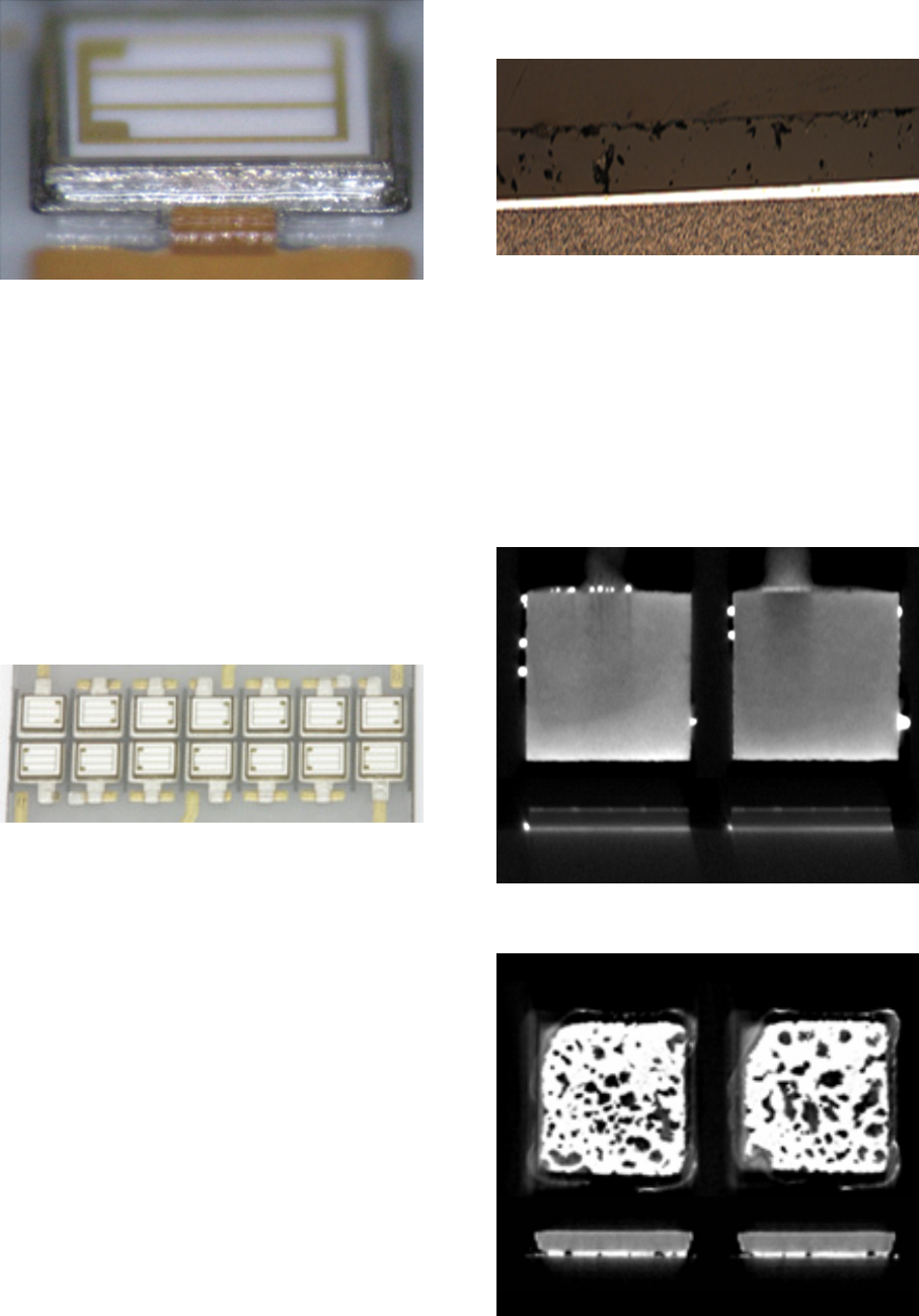
Figure 6: LED-chip soldered to an Al
2
O
3
sub-
strate.
Relevant process parameters are temperature profile
and reflow regime as well as bonding force (applied
pressure during placement and reflow). More than
30 assemblies using testing elements are manufac-
tured for mechanical testing and process optimi-
zation. Soldering of chips using less than 10 µm
sputtered AuSn layers (as-sputtered, without addi-
tional solder applied) did not prove to be reliable
joined. Low shear forces and unregular wetting are
observed. An additional Ø300 µm solder sphere is
applied to provide for an additional solder layer
thickness of 12 µm. Fully operational 7×2-chip
samples are made for optical testing (Figure 7).
Figure 7: Fully assembled 7×2 UV-LED module.
The third die-attach technology used is adhesive
bonding with silver-loaded and thermally con-
ductive adhesives. Although being a well estab-
lished and commercially used technology the appli-
cation of highly filled adhesives requires major
adaptations of dispense and chip placement techno-
logies. The optimization of the process flow, curing
conditions and homogenization of the adhesive is
necessary to achieve reproducible thin joint fis-
sures.
Experimental – Analysis of Solder Joints
Mechanical testing of soldered components, both
LED-chips and testing vehicles is conducted using
shear force measurements. Using components with
an additional solder volume, 6 N to 18 N with glass
testing elements for variation of process parameters
are achieved. LED-chips show a shear force greater
than 10 N with the main failure mode being the
rupture of chips rather than failure of solder joints
or layer interfaces. Cross section views (Figure 8)
show a homogenous filling and a solder layer thick-
ness below 30 µm.
Figure 8: Cross section view of a AuSn soldered
LED-chip.
Micro-Computer-Tomography (Micro-CT) analysis
confirms a void free and homogenous solder layer
for AuSn soldering (Figure 9). In comparison the
micro-CT shows significant voiding for the vacuum
soldered LED-chips (Figure 10). The increase of
thermal resistance of solder joints with a higher
fraction of voids is obvious. Flux-free processing of
gold-tin solder furthermore eliminates the need for
additional cleaning after soldering.
Figure 9: Micro-CT of AuSn soldered LED-
chips.
Figure 10: Micro-CT of SnPb soldered LED-
chips.
IMAPS/ACerS 8th International CICMT Conference and Exhibition (2012) | April 16-19, 2012 | Erfurt, Germany
000242
Downloaded from http://meridian.allenpress.com/imaps-conferences/article-pdf/2012/CICMT/000238/2360912/cicmt-2012-tp61.pdf by guest on 03 January 2023