67021-ultraviolet-led-multi-chip-module-based-on-ceramic-substrate.pdf - 第6页
Optical M easurements Optical po wer mea surements and wavelength s hift are o bserved using an integra ting sp here. A set up o f an Ulbricht sphere that allows for the mounting of the prop osed ceramics s ubstrate atta…
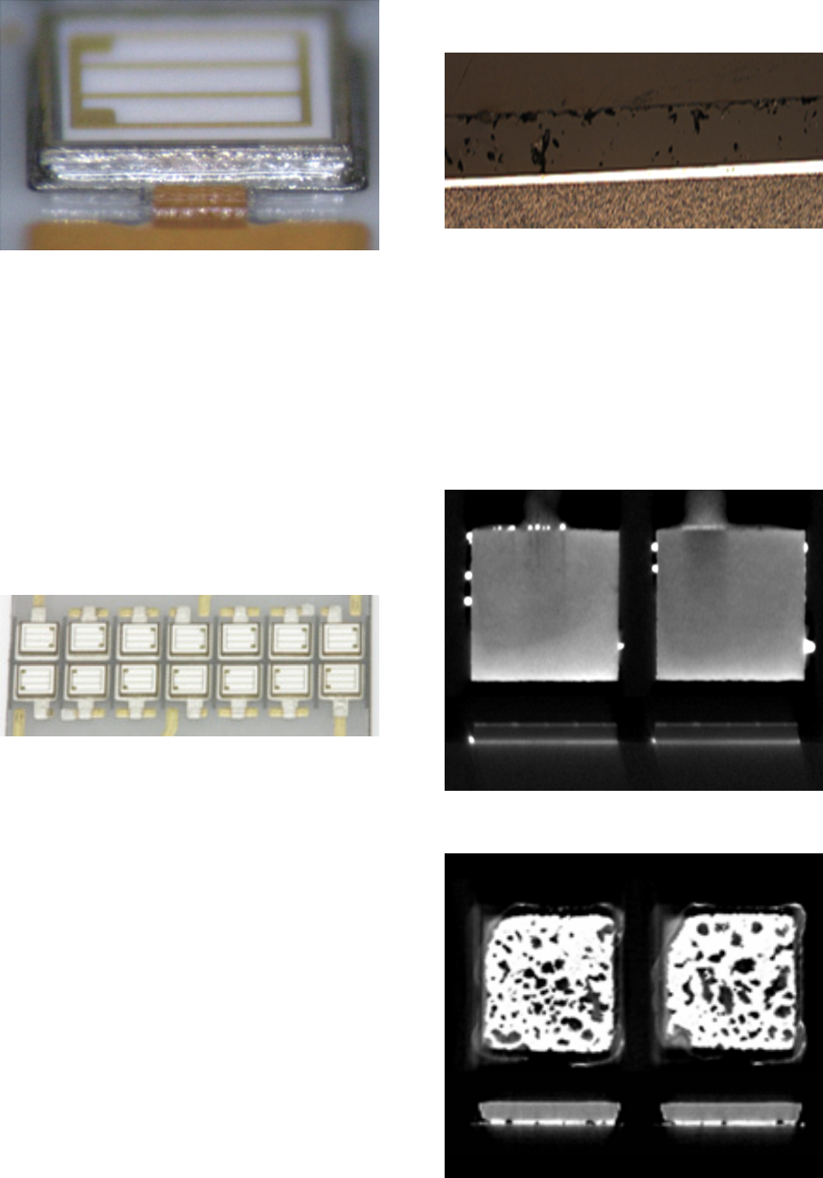
Figure 6: LED-chip soldered to an Al
2
O
3
sub-
strate.
Relevant process parameters are temperature profile
and reflow regime as well as bonding force (applied
pressure during placement and reflow). More than
30 assemblies using testing elements are manufac-
tured for mechanical testing and process optimi-
zation. Soldering of chips using less than 10 µm
sputtered AuSn layers (as-sputtered, without addi-
tional solder applied) did not prove to be reliable
joined. Low shear forces and unregular wetting are
observed. An additional Ø300 µm solder sphere is
applied to provide for an additional solder layer
thickness of 12 µm. Fully operational 7×2-chip
samples are made for optical testing (Figure 7).
Figure 7: Fully assembled 7×2 UV-LED module.
The third die-attach technology used is adhesive
bonding with silver-loaded and thermally con-
ductive adhesives. Although being a well estab-
lished and commercially used technology the appli-
cation of highly filled adhesives requires major
adaptations of dispense and chip placement techno-
logies. The optimization of the process flow, curing
conditions and homogenization of the adhesive is
necessary to achieve reproducible thin joint fis-
sures.
Experimental – Analysis of Solder Joints
Mechanical testing of soldered components, both
LED-chips and testing vehicles is conducted using
shear force measurements. Using components with
an additional solder volume, 6 N to 18 N with glass
testing elements for variation of process parameters
are achieved. LED-chips show a shear force greater
than 10 N with the main failure mode being the
rupture of chips rather than failure of solder joints
or layer interfaces. Cross section views (Figure 8)
show a homogenous filling and a solder layer thick-
ness below 30 µm.
Figure 8: Cross section view of a AuSn soldered
LED-chip.
Micro-Computer-Tomography (Micro-CT) analysis
confirms a void free and homogenous solder layer
for AuSn soldering (Figure 9). In comparison the
micro-CT shows significant voiding for the vacuum
soldered LED-chips (Figure 10). The increase of
thermal resistance of solder joints with a higher
fraction of voids is obvious. Flux-free processing of
gold-tin solder furthermore eliminates the need for
additional cleaning after soldering.
Figure 9: Micro-CT of AuSn soldered LED-
chips.
Figure 10: Micro-CT of SnPb soldered LED-
chips.
IMAPS/ACerS 8th International CICMT Conference and Exhibition (2012) | April 16-19, 2012 | Erfurt, Germany
000242
Downloaded from http://meridian.allenpress.com/imaps-conferences/article-pdf/2012/CICMT/000238/2360912/cicmt-2012-tp61.pdf by guest on 03 January 2023
Optical Measurements
Optical power measurements and wavelength shift
are observed using an integrating sphere. A setup of
an Ulbricht sphere that allows for the mounting of
the proposed ceramics substrate attached to a heat
sink is constructed. This structure permits the oper-
ation of the LED-chips at high power ratings while
diffusing the light for an integrating measurement
of total power without concerns about the direc-
tional characteristics of the LED assembly. The de-
sign of the heat-sink and the substrate clamping
lead to approx. 30% NA-loss during measurements.
A calibration of the Ulbricht sphere with respect to
this fact is used to correct the results.
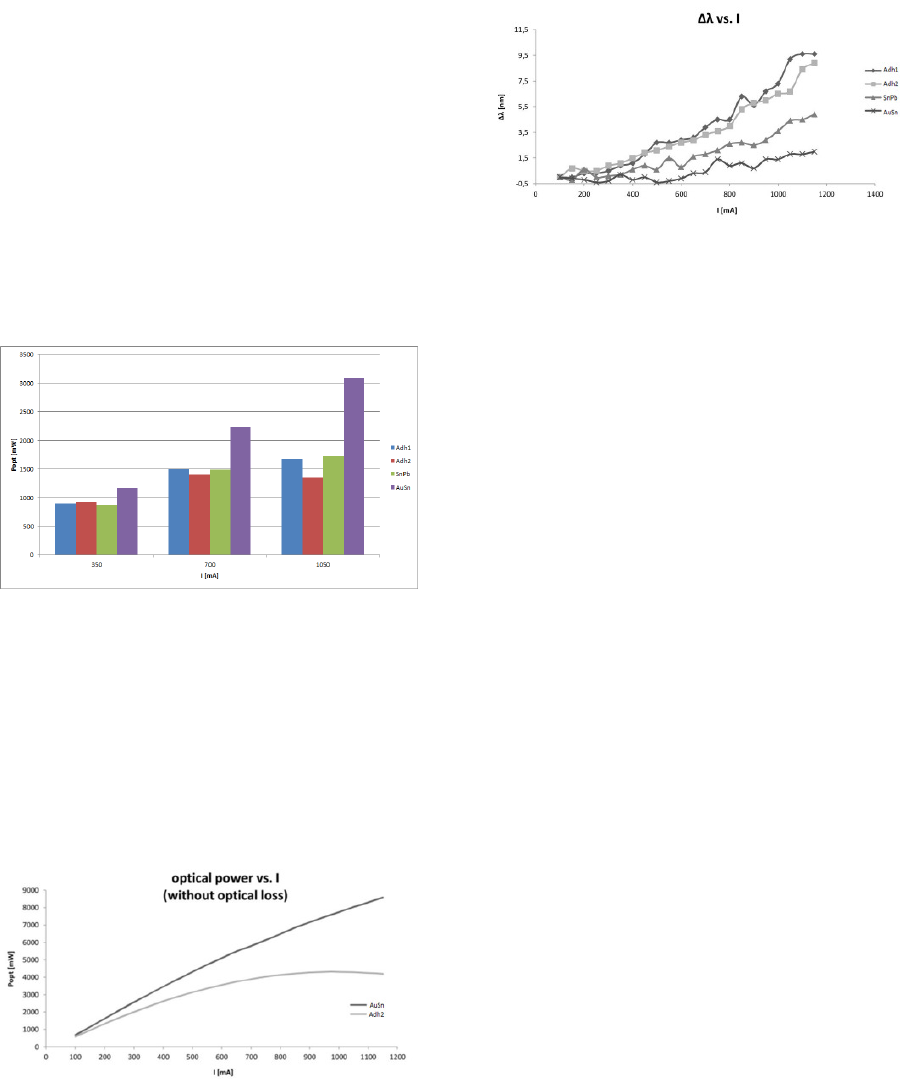
The results of optical output power of the four die-
attach variants – adhesive 1, adhesive 2, SnPb
solder, and AuSn solder – are shown in Figure 11.
Measurement has been conducted using one chan-
nel of 1×7 chips per substrate and for operational
currents of 350 mA, 700 mA and 1050 mA. A sig-
nificant improvement of output power is observed
for AuSn die-attach. Adhesive 2 shows a decrease
of output power with increased current.
Figure 11: Optical output power of one channel
(1×7 chips) for four die-attach variants.
Using both channels of 2×7 chips an optical output
power of 7.7 W is achieved at 1050 mA for AuSn
soldered assemblies. The resulting peak irradiance
is 30.8 W/cm² at the LED surface with respect to
the footprint and pitch of the attached chips. The
optimized cooling of AuSn-soldered LED-chips is
demonstrated by the increased optical output power
compared to adhesively joined LEDs (Figure 12).
Figure 12: Optical output power of both
channels (2×7 chips) for the gold-tin solder
(AuSn) and adhesive (Adh2) die-attach.
Additionally the thermally induced shift of emis-
sion wavelength can be used to compare different
die-attach technologies with respect to thermal
transfer capabilities. Better cooling corresponds to a
lower chip temperature and thus to a lower wave-
length shift. Both soldering techniques show
improved behavior compared to the adhesives
(Figure 13). Gold-tin solder layers show a lower
drift than the void-prone SnPb solder.
Figure 13: Wavelength shift over current for
four die-attach variants.
Summary and Outlook
The assembly of a UV-LED multi-chip module
using different die-attach technologies has been
demonstrated. Finite element analysis proves ac-
ceptable thermo-mechanical stresses and the reali-
zation of thermally high conductive joints using
solder alloys and new highly conductive silver-
loaded adhesives if thin layers could be processed.
The design of a multi-chip sub-module is flexible
and versatile to use. Line-shaped light sources are
possible by stackable modules. A six-module
assembly is demonstrated. Easy scaling of optical
output power as well as a simplified servicing by
changing single modules add to the customer
benefit. Measurements of optical output power and
low thermally induced wavelength drift as well as
analysis of solder layer structure show the
performance of thin gold-tin solder layers. A 14
chip module attains 7.7 W optical output power and
a respective peak irradiance of 30.8 W/cm². Long
term behavior and the investigation of reliability
over life time are the next steps to confirm the
usability of the proposed module design and die-
attach technologies.
Acknowledgements
The work presented in this paper was funded by the
TAB (Thüringer Aufbaubank) with funds provided
through EFRE (Europäische Fonds für regionale
Entwicklung) OP 2007-2013 under project FK
2009VF0003. The authors would like to thank G.
Leibeling, T. Feigl and A. Joswig for sample prepa-
ration, P. Kühmstedt for micro-tomography ana-
lysis and R. Schmidt for equipment manufacturing.
IMAPS/ACerS 8th International CICMT Conference and Exhibition (2012) | April 16-19, 2012 | Erfurt, Germany
000243
Downloaded from http://meridian.allenpress.com/imaps-conferences/article-pdf/2012/CICMT/000238/2360912/cicmt-2012-tp61.pdf by guest on 03 January 2023
References
[1] M.S. Shur, R. Gaska, “Deep-Ultraviolet Light-
Emitting Diodes”, IEEE Trans. Electron De-
vices, Vol. 57, Num. 1, pp. 12 – 25, Jan 2010;
doi:10.1109/ TED.2009.2033768.
[2] S.L. McDermott, J.E. Walsh, R.G. Howard,
“A comparison of the emission characteristics
of UV-LEDs and fluorescent lamps for poly-
merisation applications”, Optics & Laser
Technology 40 (2008) 487 – 493; doi:10.
1016/j.optlastec.2007.07.013.
[3] M. Schneider, C. Herbold, K. Messerschmidt,
K. Trampert, J. J. Brandner, “High power UV-
LED-clusters on ceramic substrates”, Electro-
nic Components and Technology Conference
(ECTC), 2010 Proceedings 60
th
, pp. 679 –
685, June 2010; doi: 10.1109/ECTC.2010.
5490793.
[4] J.K. Park, H.D. Shin, Y.S. Park, S.Y. Park,
K.P. Hong, B.M. Kim, “A suggestion for high
power LED package based on LTCC”, Elec-
tronic Components and Technology Confe-
rence (ECTC), 2006, Proceedings 56
th
; doi:10.
1109/ ECTC.2006.1645786.
[5] M.A. Würtele, T. Kolbe, M. Lipsz, A. Kül-
berg, M. Weyers, M. Kneisel, M. Jekel,
„Application of GaN-based ultraviolet-C light
emitting diodes – UV LEDS – for water dis-
infection“, Water Research 45 (2011) 1481 –
1489; doi:10.1016/j.watres.2010.11.015.
[6] Liao, C. Thomidis, C. Kao, T. Moustakas,
“AlGaN based deep ultraviolet light emitting
diodes with high internal quantum efficiency
grown by molecular beam epitaxy”, Appl.
Phys. Lett. 98, 081110 (2011); doi:10.1063/
1.3559842.
[7] M. Kneisel, T. Kolbe, C. Chua, V. Kueller, N.
Lobo, J. Stellmach, A. Knauer, H. Rodriguez,
S. Einfeldt, Z. Yang, N.M. Johnson, M.
Weyers, “Advances in group III-nitride-based
deep UV light-emitting diode technology”,
Semicond. Sci. Technol. 26 (2011) 014036;
doi:10.1088/0268-1242/26/1/014036.
[8] K.T. Lam, S.C. Hung, C.F. Shen, C.H. Liu,
Y.X. Sun, S.J. Chang, “Effects of the sapphire
substrate thickness on the performances of
GaN-based LEDs”, Semicond. Sci. Technol.
24 (2009) 065002; doi:10.1088/0265-1242/24/
6/065002.
[9] R.W. Chuang, D. Kim, J. Park, C.C. Lee, “A
fluxless process of producing tin-rich gold-tin
joints in air”, Components and Packaging
Technologies, IEEE Transactions on, Vol. 27,
No. 1, (2004), pp. 177 – 181; doi:10.1109/
TCAPT.2004.825757.
[10] H. Banse, R. Eberhardt, E. Beckert, W.
Stöckl, „Laser Beam Soldering – a New
Assembly Technology for Microoptical
Systems“, Microsystem Technologies 11
(2005) 186 – 193; doi:10.1007/s00542-004-
0451-y.
[11] M. Rettenmayr, P. Lambracht, B. Kempf, M.
Graff, „High Melting Pb-Free Solder Alloys
for Die-Attach Applications“, Advanced
Engineering Materials, 7: 965 – 969; doi:10.
1002/adem.200500124.
[12] L. Guo-Quan, J.N. Calata, Z. Zhiye, J.G. Bai,
“A lead-free, low-temperature sintering die-
attach technique for high-performance and
high-temperature packaging”, High Density
Microsystems Design and Packaging and
Component Failure Analysis, 2004, Procee-
dings of the 6
th
IEEE CPMT Conference on,
Jun 2004, pp. 42 – 46; doi:10.1109/ HPD.
2004.1346671.
[13] W. Schmitt, “New silver contact pastes from
high pressure sintering to low pressure sin-
tering”, Electronic System-Integration Tech-
nology Conference (ESTC), Sept. 2010; doi:
10.1109/ESTC.2010.5642933.
[14] T. Aalto, M. Harjanne, M. Kapulainen, S.
Ylinen, J. Ollila, V. Vilokkinen, L. Mörl, M.
Möhrle, R. Hamelin, “Integration of InP-based
optoelectronics with silicon waveguides”,
Proc. SPIE 7218, 72180O (2009); doi:10.
1117/12.808129.
[15] G. Caswell, “NanoBond® Assembly – A rap-
id, room temperature soldering process”,
European Microelectronics and Packaging
Conference EMPC, June 2009.
[16] A.J. Swiston Jr., T.C. Hufnagel, T.P. Weihs,
“Joining bulk metallic glass using reactive
multilayer foils”, Scripta Materialia, Vol. 48,
No. 12, (2003), pp. 1575 – 1580; doi:10.1016/
S1359-6462(03)00164-7.
[17] S.K. Kang, R.S. Rai, S. Purushothaman, „De-
velopment of High Conductivity Lead (Pb)-
Free Conducting Adhesives“, IEEE Trans-
actions on Components, Packaging, and
Manufacturing Technology A, Vol. 21, No. 1,
(1998), pp. 18 – 22; doi:10.1109/95.679027.
[18] D. Lu, C. Liu, X. Lang, B. Wang, Z. Li,
W.M.P. Lee, S.W.R. Lee, „Enhancement of
thermal conductivity of die attach adhesives
(DAAs) using nanomaterials for high bright-
ness light-emitting diode (HBLED)”, Electro-
nic Components and Technology Conference
(ECTC), 2011 Proceedings 61
st
; doi:10.1109/
ECTC.2011.5898585.
[19] V.R. Manikam, K.Y. Cheong, “Die attach
materials for high temperature applications: A
IMAPS/ACerS 8th International CICMT Conference and Exhibition (2012) | April 16-19, 2012 | Erfurt, Germany
000244
Downloaded from http://meridian.allenpress.com/imaps-conferences/article-pdf/2012/CICMT/000238/2360912/cicmt-2012-tp61.pdf by guest on 03 January 2023