IPC7527-2012RequirementsforSolderPastePrinting.pdf - 第13页
5.1.3 Solder Paste Deposit – Area It may be necessary to use a measurement system to evaluate this factor . See Section 4, MEASUREMENT OF SOLDER P ASTE DEPOSITS. Target – Class 1, 2, 3 • Coverage = 100% of stencil apertu…
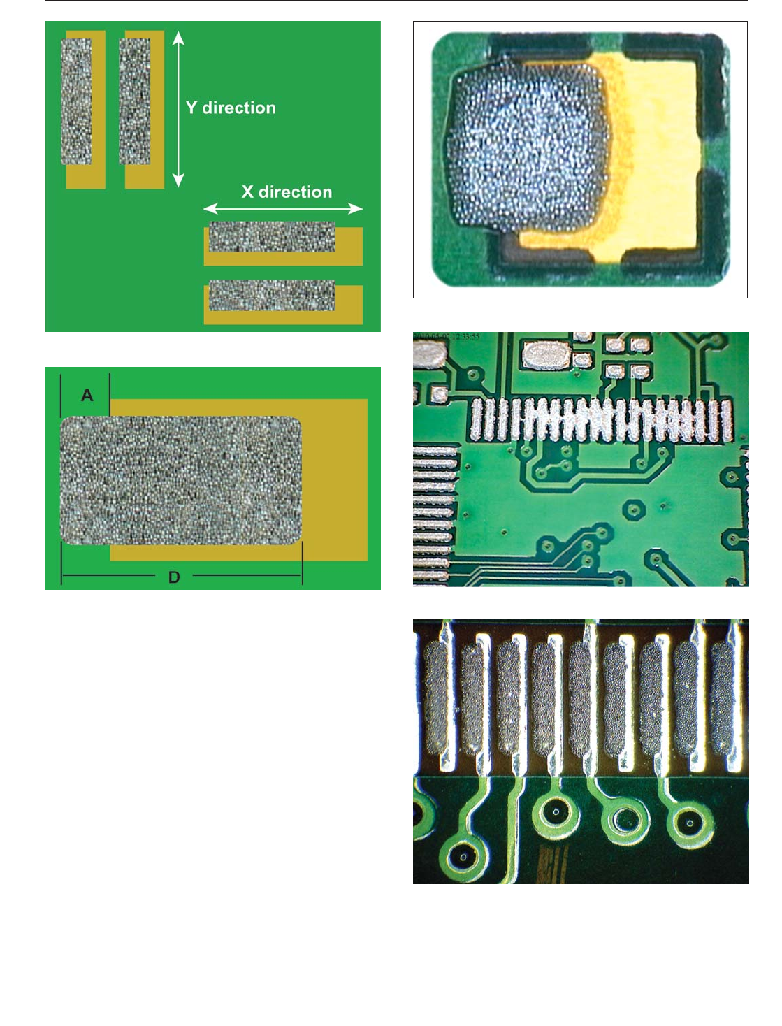
Defect – Class 1, 2, 3
• Solder paste deposit has connected with adjacent pad
(Figure 5-15).
• Paste deposit (D) is off pad >25% (A) in X and/or Y
direction (Figures 5-14 through 5-16).
• Solder deposit not in single block (except by design).
• Solder balls that do not contact the solder paste deposit.
Figure 5-12 Offset – Acceptable
Figure 5-13 Offset – Acceptable
Figure 5-14 Offset – Defect
Figure 5-15 Shorting – Defect
Figure 5-16 Offset – Defect
IPC-7527 May 2012
6
Copyright IPC-Association Connecting Electronics Industries
Provided by IHS under license with IPC
Not for Resale
No reproduction or networking permitted without license from IHS
--`,,```,,,,````-`-`,,`,,`,`,,`---
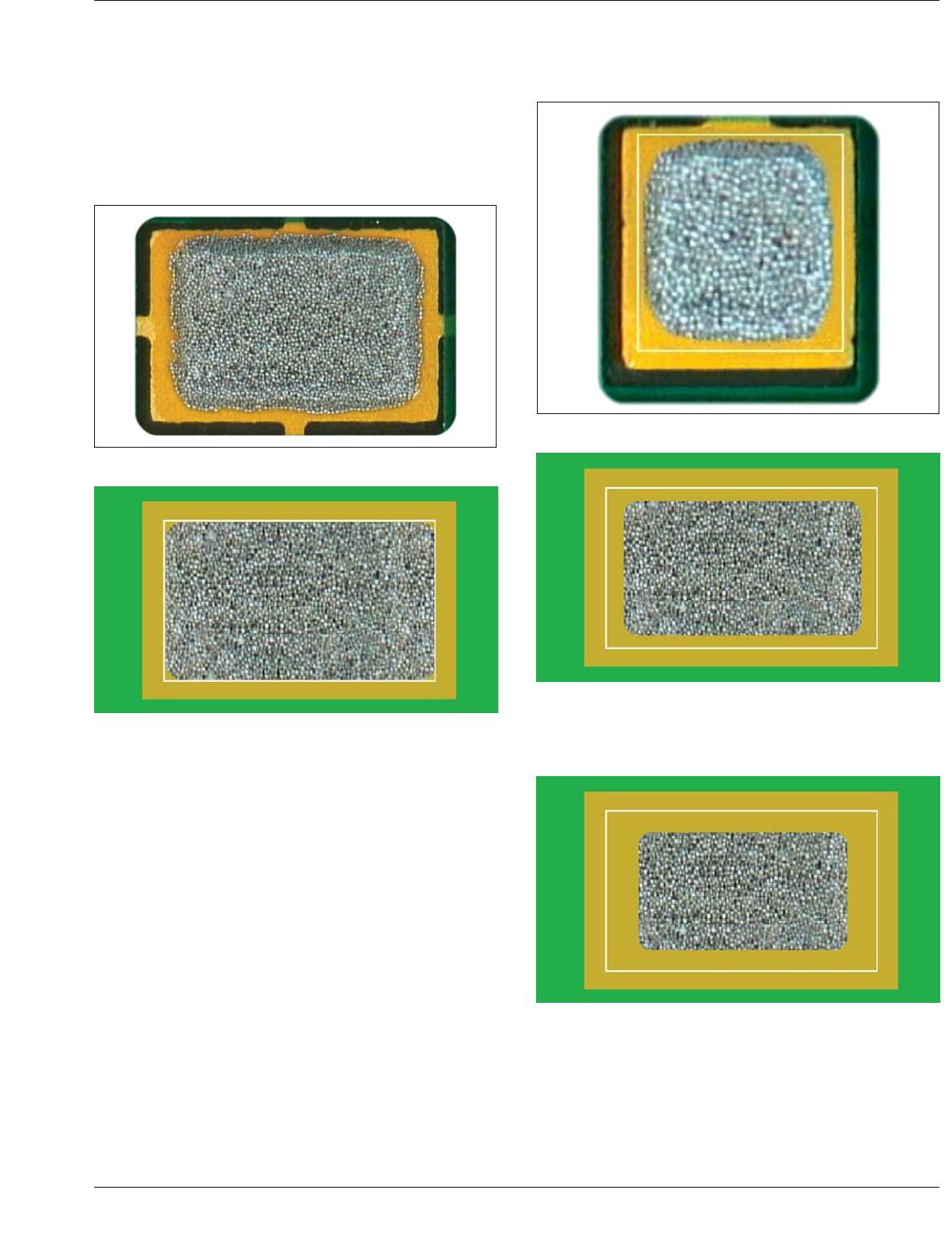
5.1.3 Solder Paste Deposit – Area It may be necessary
to use a measurement system to evaluate this factor. See
Section 4, MEASUREMENT OF SOLDER PASTE
DEPOSITS.
Target – Class 1, 2, 3
• Coverage = 100% of stencil aperture (Figures 5-17 and
5-18).
Process Indicator – Class 1, 2, 3
• Coverage 75% of stencil aperture (Figures 5-19 and
5-20).
Defect – Class 1, 2, 3
• Coverage <50% of stencil aperture (Figure 5-21).
Figure 5-17 Area – Target
Figure 5-18 Area – Target
Figure 5-19 Area – Acceptable
Figure 5-20 Area – Acceptable
Figure 5-21 Area – Defect
May 2012 IPC-7527
7
Copyright IPC-Association Connecting Electronics Industries
Provided by IHS under license with IPC
Not for Resale
No reproduction or networking permitted without license from IHS
--`,,```,,,,````-`-`,,`,,`,`,,`---
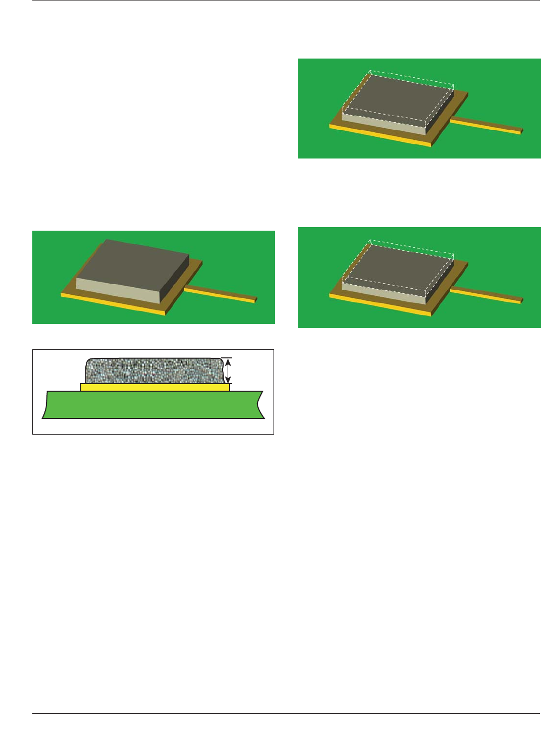
5.1.4 Solder Paste Deposit – Height It may be neces-
sary to use a measurement system to evaluate this factor.
See Section 4, MEASUREMENT OF SOLDER PASTE
DEPOSITS.
Example of Tolerance:
• Component pin co-planarity: 100 µm [0.0039 in]
• Stencil thickness: 127 µm [0.005 in]
• Reduction of 20%
• Result of theoretical paste deposit height: 102 µm
[0.004 in]
See Appendix A for further examples.
Target – Class 1, 2, 3
• Nominal height is achieved, (deposit height = stencil
thickness) (Figures 5-22 and 5-23).
Process Indicator – Class 1, 2, 3
• Paste deposit height 75% of stencil thickness (Figure
5-24).
Defect – Class 1, 2, 3
• Paste deposit height 50% of stencil thickness (Figure
5-25).
Figure 5-22 Height – Target
IPC-7527-5-23
Figure 5-23 Height – Target
Figure 5-24 Height – Process Indicator
Figure 5-25 Height – Defect
IPC-7527 May 2012
8
Copyright IPC-Association Connecting Electronics Industries
Provided by IHS under license with IPC
Not for Resale
No reproduction or networking permitted without license from IHS
--`,,```,,,,````-`-`,,`,,`,`,,`---