IPC7527-2012RequirementsforSolderPastePrinting.pdf - 第9页
4 MEASUREMENT OF SOLDER PASTE DEPOSITS V arious types of equipment can be used to measure the solder paste print. The measurement can be done manually or with an automatic inspection system. Figures 4-1 and 4-2 illustrat…
Whenever possible these criteria should be submitted to the
IPC Technical Committee to be considered for inclusion in
upcoming revisions of this standard.
1.6 Verification of Dimensions The actual measure-
ments provided in this document (i.e., specific part mount-
ing and solder fillet dimensions and determination of per-
centages) are not required except for referee purposes. All
dimensions in this standard are expressed in SI (System
International) units (with Imperial English equivalent
dimensions provided in brackets). All specified limits in
this standard are absolute limits as defined in ASTM E29.
1.7 Magnification Aids For visual inspection, some indi-
vidual specifications may call for magnification aids for
examining solder paste print.
The tolerance for magnification aids is ± 15% of the
selected magnification power. Magnification aids, if used
for inspection, shall be appropriate for the item being
inspected. Unless magnification requirements are otherwise
specified by contractual documentation, the magnifications
in Table 1-1 are determined by the item being inspected.
Referee conditions are used to verify product rejected at
the inspection magnification power. For assemblies with
mixed land widths, the greater magnification may be used
for the entire assembly.
1.8 Lighting Lighting shall be adequate for the item
being inspected.
Illumination at the surface of workstations should be at
least 1000 lm/m
2
[approximately 93 foot candles]. Light
sources should be selected to prevent shadows.
Note: In selecting a light source, the color temperature of
the light is an important consideration. Light ranges from
3000-5000° K enable users to distinguish various solder
paste printing features and contaminates with increased
clarity.
2 APPLICABLE DOCUMENTS
The following documents currently in effect form a part of
this specification to the extent specified herein.
2.1 IPC
1
IPC-J-STD-005 Requirements for Soldering Pastes
IPC-HDBK-005 Guide to Solder Paste Assessment
IPC-T-50 Terms and Definitions for Interconnecting and
Packaging Electronic Circuits
IPC-A-610 Acceptability of Electronic Assemblies
IPC-7525 Stencil Design Guidelines
IPC-7526 Stencil and Misprinted Board Cleaning Hand-
book
2.2 ASTM
2
ASTM E29 Standard Practice for Using Significant Digits
in Test Data to Determine Conformance with Specifica-
tions.
3 CHOICE OF TECHNOLOGY
The requirements in this standard have been developed for
solder paste printing. Since the requirements are referred to
as general, it is also possible to evaluate other application
methods according to this standard. However, it may be
necessary to develop specific acceptance requirements for
the chosen application method.
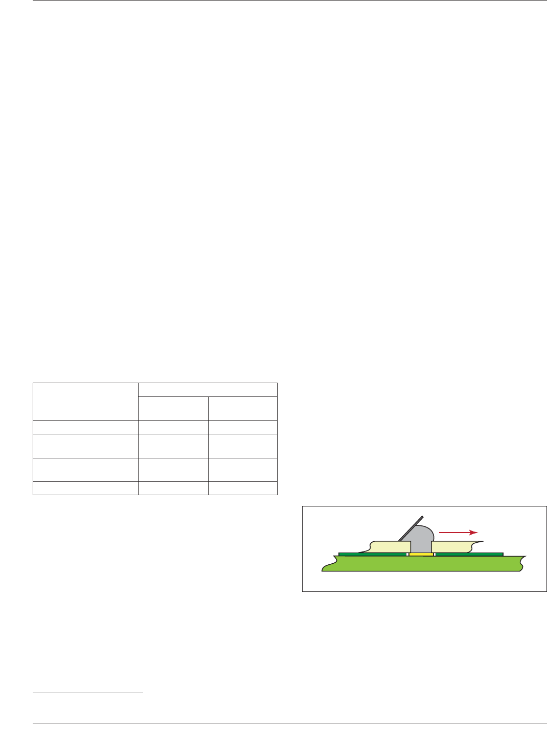
Various methods can be used when solder paste is applied
to the PCB (printed circuit board). Four methods are illus-
trated here:
• Squeegee Blade (Figure 3-1)
• Enclosed Print Head (Figure 3-2)
• Needle Dispense (Figure 3-3)
• Paste Jet Dispense (Figure 3-4)
1. www.ipc.org
2. www.astm.org
Table 1-1 Inspection Magnification (Land Width)
Land Widths or
Land Diameters
Magnification Power
Inspection
Range
Maximum
Referee
>1.0 mm [0.0394 in] 1.5X to 3X 4X
>0.5 to ≤1.0 mm
[0.0197 to 0.0394 in]
3X to 7.5X 10X
≥0.25 to ≤0.5 mm
[0.00984 to 0.0197 in]
7.5X to 10X 20X
<0.25 mm [0.00984 in] 20X 40X
IPC-7527-3-1
Figure 3-1 Squeegee Blade
1. Squeegee
2. Paste
3. Stencil
4. PCB
1
23
4
IPC-7527 May 2012
2
Copyright IPC-Association Connecting Electronics Industries
Provided by IHS under license with IPC
Not for Resale
No reproduction or networking permitted without license from IHS
--`,,```,,,,````-`-`,,`,,`,`,,`---
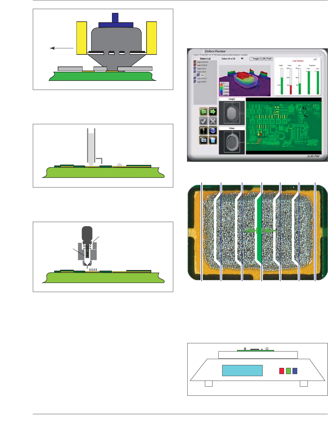
4 MEASUREMENT OF SOLDER PASTE DEPOSITS
Various types of equipment can be used to measure the
solder paste print. The measurement can be done manually
or with an automatic inspection system. Figures 4-1 and
4-2 illustrate the results from two automated methods of
paste measurement. It is often necessary to perform mea-
surements in order to control the amount of solder paste.
This paragraph is not a step by step process requirement,
but an overview of technologies that can be implemented
when measuring the amount of solder paste.
Follow the manufacturer’s instructions when using auto-
mated measuring equipment. Each automated inspection
equipment manufacturer may use different equations to
determine height, area, and volume of the solder deposit. It
is up to the user of this standard to translate from this
guideline to the individual automated inspection equip-
ment.
Controlling the amount by weighing the PCB shows the
total amount of solder paste on the board (Figure 4-3). By
comparing the result with a PCB, with a correct amount of
solder paste, you will get an exact indication of potential
deviance.
IPC-7527-3-2
Figure 3-2 Enclosed Paste Print Head
1. Enclosed Paste Head
2. Stencil
3. PCB
1
3
2
IPC-7527-3-3
Figure 3-3 Needle Dispense
1. PCB
2. Needle Dispenser
3. Paste Deposit
1
2
3
IPC-7527-3-4
Figure 3-4 Paste Jet Dispense
1. Motor
2. Paste
3. Paste Deposit
4. PCB
4
3
2
1
Figure 4-1 Sample of an Automated Machine Readout
(Screen Capture Courtesy of CyberOptics Corporation)
Figure 4-2 Sample of an Automated Inspection Result
(Image Courtesy of HYTEK)
IPC-7527-4-3
Figure 4-3 Weighing Solder Paste
4.021
g
May 2012 IPC-7527
3
Copyright IPC-Association Connecting Electronics Industries
Provided by IHS under license with IPC
Not for Resale
No reproduction or networking permitted without license from IHS
--`,,```,,,,````-`-`,,`,,`,`,,`---
Control of the deposited amount ensures that the design
amount is obtained with reference to the thickness and
aperture of stencil. However, total weight of the assembly
cannot take the place of measurement of individual paste
deposits. Weight is only used for total volume assessment.
To weigh the boards, weigh clean, bare boards. Deposit the
paste using the normal print process. Then weigh the same
board again to determine the difference between the clean
board and the printed board. The difference will be the total
volume of paste applied to the board.
It is recommended to use a calibrated and accurate scale.
The accuracy of the scale will be determined according to
the size and density of the board assembly.
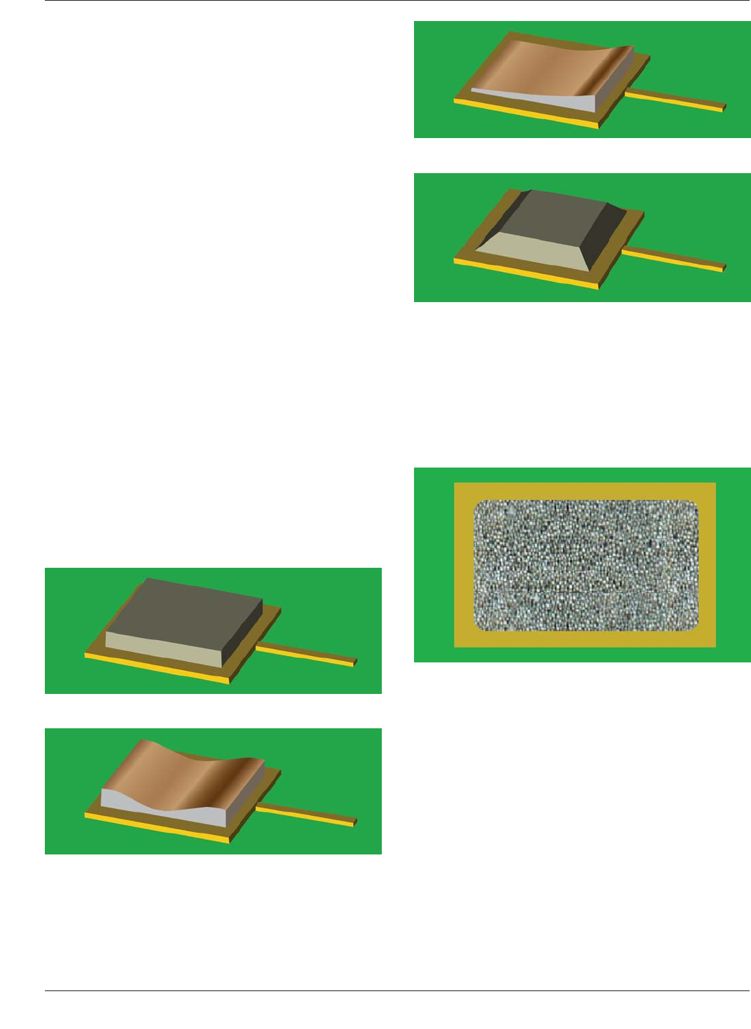
5 SHAPE OF SOLDER PASTE DEPOSIT
The volume and placement precision of the solder paste
deposits are the important factors for a correct solder paste
deposit. Ideally the paste deposit should have the same
shape as the stencil aperture (area and height). However, to
some extent it will be acceptable with varying paste deposit
shapes. See the appendix for possible shapes.
The paste deposit shape can be defined as follows:
• Full Shape (Figure 5-1)
• Saddle Shape (Figure 5-2)
• Roof Top Shape (Figure 5-3)
• Pyramid Shape (Figure 5-4)
5.1 Solder Paste Deposit – Misalignment A process
control system is recommended to ensure the lowest pos-
sible error rate, e.g., Statistical Process Control (SPC).
5.1.1 Slump
Target – Class 1, 2, 3
• Full shape solder paste deposit (Figure 5-5).
Acceptable – Class 1
• The paste deposit deviates from the nominal shape but
has the designed shape and volume.
Acceptable – Class 2, 3
• The paste deposit deviates from the designed shape but
slumps less than 25% in the X and Y directions.
Defect – Class 1
• Paste has connected with adjacent deposits.
Defect – Class 2, 3
• The paste has slumped more than 25% in the X and/or Y
directions.
Figure 5-1 Full Shape
Figure 5-2 Saddle Shape
Figure 5-3 Roof Top Shape
Figure 5-4 Pyramid Shape
Figure 5-5 Full Shape
IPC-7527 May 2012
4
Copyright IPC-Association Connecting Electronics Industries
Provided by IHS under license with IPC
Not for Resale
No reproduction or networking permitted without license from IHS
--`,,```,,,,````-`-`,,`,,`,`,,`---