(TI)对半导体器件的长期存储评估.pdf - 第11页
Figure 1 1-14. Lead Side View After Bake Figure 1 1-15. Lead Side View After Soldering 1 1.3 SOIC (Small Outline Integrated Circuit) Sample batch #46: 21 years storage, MSL1, SOIC D, lead finish : pre-plated NiPdAu Figur…
11.2 SOT (Small Outline Transistor) Package
Sample batch #30: 11 years storage, MSL2, SOT23 DCN, lead finish: post assembly Tin (Sn) plated
Figure 11-6. Unit After Bake 4hr/
150°C
Figure 11-7. Print Pattern
Figure 11-8. Bottom View After
Test
Figure 11-9. Lead Side View After
Bake
Figure 11-10. Lead Side View After
Soldering
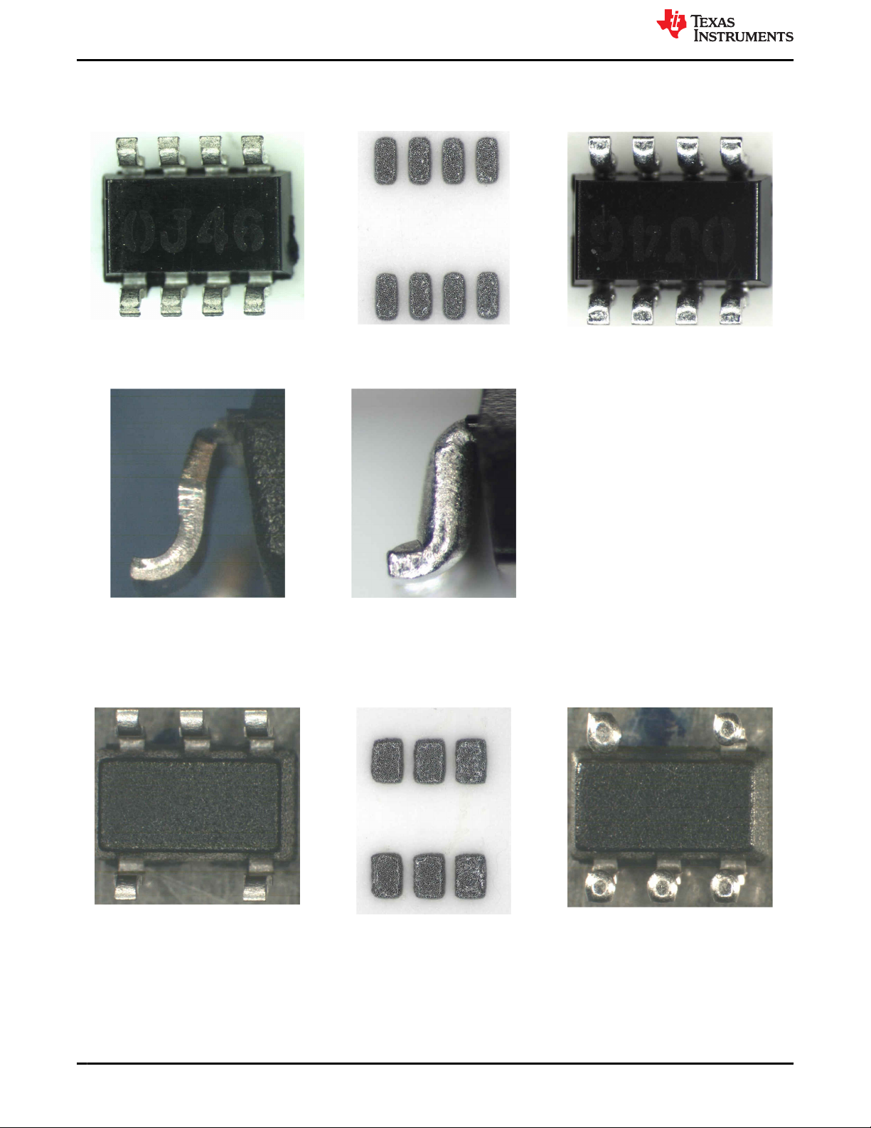
Sample batch #21: 17 years storage, MSL1, SOT23 DBV, lead finish: pre-plated NiPdAu
Figure 11-11. Unit After Bake 4hr/
150°C
Figure 11-12. Print Pattern
Figure 11-13. Bottom View After
Test
Solderability Test Results www.ti.com
10 Long Term Storage Evaluation of Semiconductor Devices SLPA019 – SEPTEMBER 2021
Submit Document Feedback
Copyright © 2021 Texas Instruments Incorporated
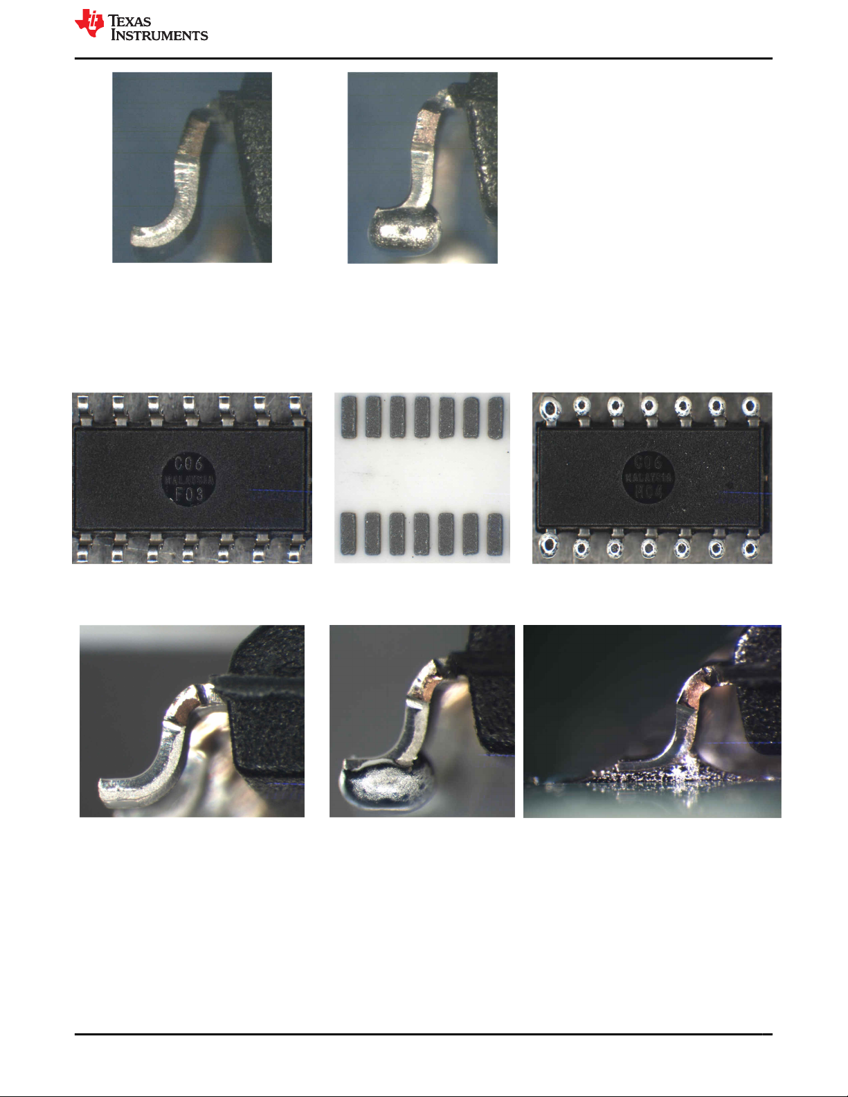
Figure 11-14. Lead Side View After
Bake
Figure 11-15. Lead Side View After
Soldering
11.3 SOIC (Small Outline Integrated Circuit)
Sample batch #46: 21 years storage, MSL1, SOIC D, lead finish: pre-plated NiPdAu
Figure 11-16. Unit After Bake 4Hr/
150°C
Figure 11-17. Solder Paste Print
Pattern
Figure 11-18. Bottom View After
Test
Figure 11-19. Lead Side View After
Bake
Figure 11-20. Lead Side View After
Soldering
Figure 11-21. Lead Side View
Soldered PCB
www.ti.com Solderability Test Results
SLPA019 – SEPTEMBER 2021
Submit Document Feedback
Long Term Storage Evaluation of Semiconductor Devices 11
Copyright © 2021 Texas Instruments Incorporated
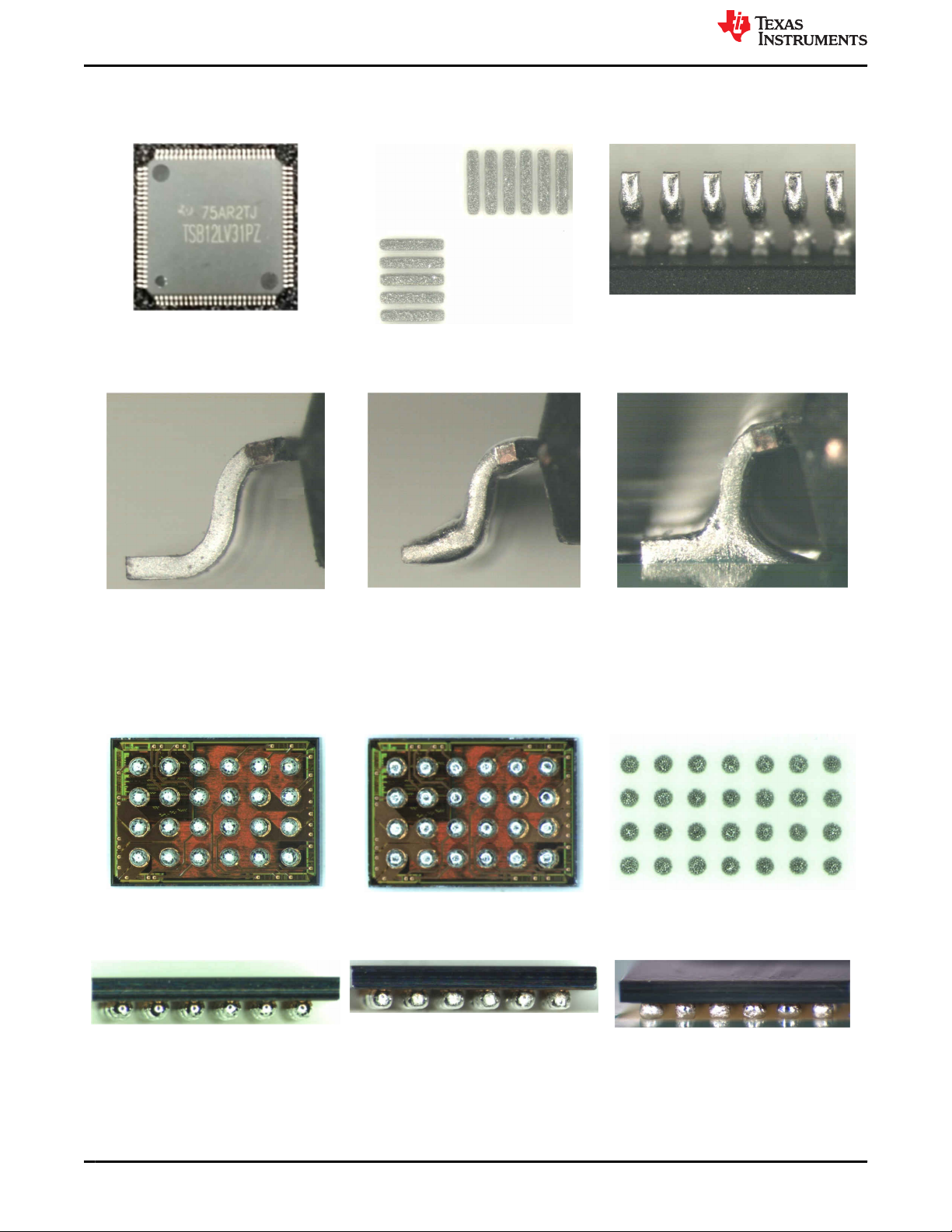
11.4 QFP (Quad Flat Pack)
Sample batch #S8: 18 years storage, MSL3, TQFP 100 pin, lead finish: post assembly plated Sn
Figure 11-22. Package Top View
Figure 11-23. Solder Past Print
Corner
Figure 11-24. Bottom View After
Test
Figure 11-25. Lead Side View
Original
Figure 11-26. Lead Side View After
Soldering
Figure 11-27. Lead Soldered on
PCB
11.5 BGA (Ball Grid Array)/WCSP (Wafer Level Chip Scale Package)
Sample Batch #38: 12 years storage, MSL1, wafer chip scale package (WCSP) 24 SnAgCu solder balls
Figure 11-28. Unit After Bake 4 hr/
150°C
Figure 11-29. Bottom View After
Test
Figure 11-30. Solder Paste Print
Pattern
Figure 11-31. Side View After Bake
Figure 11-32. Side View After
Soldering
Figure 11-33. Side View Soldered
on PCB
Solderability Test Results www.ti.com
12 Long Term Storage Evaluation of Semiconductor Devices SLPA019 – SEPTEMBER 2021
Submit Document Feedback
Copyright © 2021 Texas Instruments Incorporated