ENG_SS_108-90807_C.pdf
Product Specification 108 - 9080 7 08-A pr- 20 Rev . C ....................................................................................................................... .............................................…
Product Specification
108-90807
08-Apr-20 Rev. C
..................................................................................................................................................................................................................................…………………………….
DR. Bart Kerckhof DATE 08 apr-20
APVD. Jan Van Cauwenberge
DATE 08 apr-20
© 2020 TE Connectivity family of
companies
All Rights Reserved
*Trademark. TE Connectivity, TE connectivity (logo), and TE (logo)
are trademarks. Other logos, product, and/or company names may
be trademarks of their respective owners.
This controlled document is subject to change.
For latest revision and Regional Customer
Service, visit our website at
www.te.com.
1 of 7
PRODUCT INFORMATION
1-800-522-6752
LOC GW
“Multispring B signal” Press-in zone for automotive use
PCB Hole size
0.97…1.03…1.07 mm
Board thickness
>=1.6 mm (nominal)
Stock thickness
0.6 … 0.64 mm
TABLE OF CONTENTS
1. Scope.
2. Printed board and hole information.
3. Press-in zone information.
4. Information on the application.
5. Instruction and tools for the press-in operation.
6. Press-in characteristics.
6.1 Mechanical.
6.2 Electrical.
6.3 Environmental.
7. Requirements.
8. Related Documents.
8.1 Test-Reports.
Product specification ‘Multispring B signal’ 108-90807
................................................................................................................................................................................................................................................…………………..
Rev. C Page 2 of 7
R1-1 (Rev. 02-00)
1. SCOPE .
This specification covers all the information as required in the IEC 60352-5 (Issue 5; 2012) for a Multispring
Press-In zone (further named “Multispring”) for nominal hole-Ø 1 mm and made from
0.6 … 0.64 mm stock thickness.
The drilled holes do not follow the IEC-specification 60352-5 and are drilled 1.10 mm instead of 1.15 mm.
Reason for this is to shift the finished hole diameter in chem. Sn PCB’s more towards the nominal value.
The IEC requirements are supplemented with the requirements for automotive use based on the
“Arbeitskreis Prüfrichtlinie für KFZ-Steckverbinder”.
2. PRINTED BOARD AND HOLE INFORMATION
Printed board material according to:
- High temperature FR4 (CTE optimized): Base material: Matsushita R1566 or Nanya NP175F / 8 mal
Prepreg 7628
Aging of PCB with 2 reflow cycles with lead free temperature profile before pin insertion
- FR4 (normal): Base material: S1000
Aging of PCB with 2 reflow cycle with lead free temperature profile before pin insertion
Other board materials possible after agreement between TE Engineering and the customer
Maximum number of conductive layers: not limited.
Printed board thickness: 1.6 ±0.14 mm and 1.5 ± 0.14 mm (without copper and solder resist)
Other smaller board thicknesses have to be tested.
Plated-Through-Hole dimensions:
Hole-Ø prior to plating = 1.10±0.03 mm
Thickness of the PTH-wall: 30...55 µm Cu
Finished hole-Ø = 1.03 +0,04 -0,06 mm
Printed board plating material:
- PCB Type A: Sn plated PCB’s:
Chemical Sn ≥ 1 µm before reflow ageing
(amount of Ag: 0.5...1.5 weight %; cpk 1.33; typical values with 3 Sigma are 1.1 μm–1.3 μm)
- PCB Type B: OSP protected PCB’s:
OSP, surface thickness 0.2μm-0.5μm, released Entek Plus HT of company Enthone or Glicoat
F2(LX) of company Shikoku.
- Other plating materials have to be tested on request.

Product specification ‘Multispring B signal’ 108-90807
................................................................................................................................................................................................................................................…………………..
Rev. C Page 3 of 7
R1-1 (Rev. 02-00)
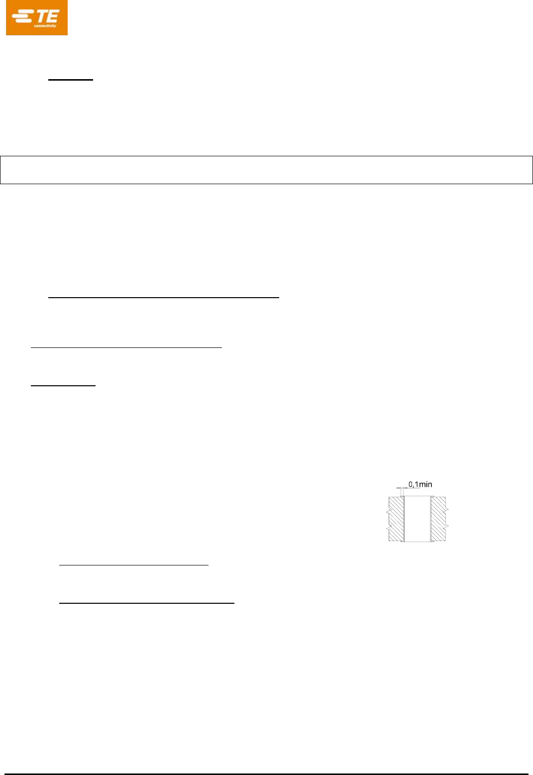
3. PRESS-IN ZONE INFORMATION
Design: see dimensional drawing on page 5
In order not to damage the PTH-hole during the press-in operation, the geometry of the guiding pin
has to be rounded and have a smooth transition to the actual multispring geometry
Stock Material:
Material Type A: CuSn6 C51900
CuSn6 UNS C51900 with tensile strength between 560-650 N/mm²
Material Type B: CuNiSi C19010
CuNiSi UNS C19010 R580s with tensile strength 580-650 N/mm²
Other materials possible after agreement between TE Engineering and the customer
Plating:
- Scenario A old measuring method SnFlash
Meant for airbag applications.
SnFlash measurement according old measuring method (before 03/2019)
0.25-0.52 µm SnPb/Sn over 1.27-2.2µm Ni. Only 1 measuring point (see page 5).
- Scenario B old measuring method SnFlash:
Meant for ABS and non-airbag applications.
SnFlash measurement according old measuring method (before 03/2019)
0.25-0.58 µm Sn over 1.27-2.2 µm Ni. 2 measuring points: (see page 5).
Target should be 0.42 µm Sn
- Scenario C new measuring method SnFlash:
Meant for new applications after 03/2019
SnFlash measurement according the new measuring method (after 03/2019)
Measurement done on 2 measuring points (see page 5)
Thickness measurement based on both sides: 0.45...0.85 μm Sn over 1.27…2.2 μm Ni.
For the first 30 minutes after new start of plating line an increased thickness of 0.45…0.90μm Sn
over 1.27…2.2μm Ni is allowed.
Thickness measurement needs to be done according to Bosch General Measurement instruction 1
279 916 072 and specific Instruction for Sn 1 279 916 073 (TE spec 129-90108).
- Scenario D old measuring method: SnEP:
Not applicable anymore (before 03/2019)
- Scenario E new measuring method: SnEP:
Meant for new applications after 03/2019
0.35 … 0.75 µm SnEP Fa. Enayati GmbH &Co KG (order specification 2 269 915 602 v02) over
1.30 …2.2 µm Ni at functional press fit zone
see drawings page 5 (2 measuring points are same as scenario B old & C new)
The surface thickness measurement of the plating has to be done according to Bosch 1 279 916
072 in general and according to Bosch 1 279 916 074 SnAg / AgSn flash coating specific.
Any temperature treatment after electroplating (for example reflow process) is not allowed without
the agreement of product engineering and customer