HS50 circuit diagram.pdf - 第84页
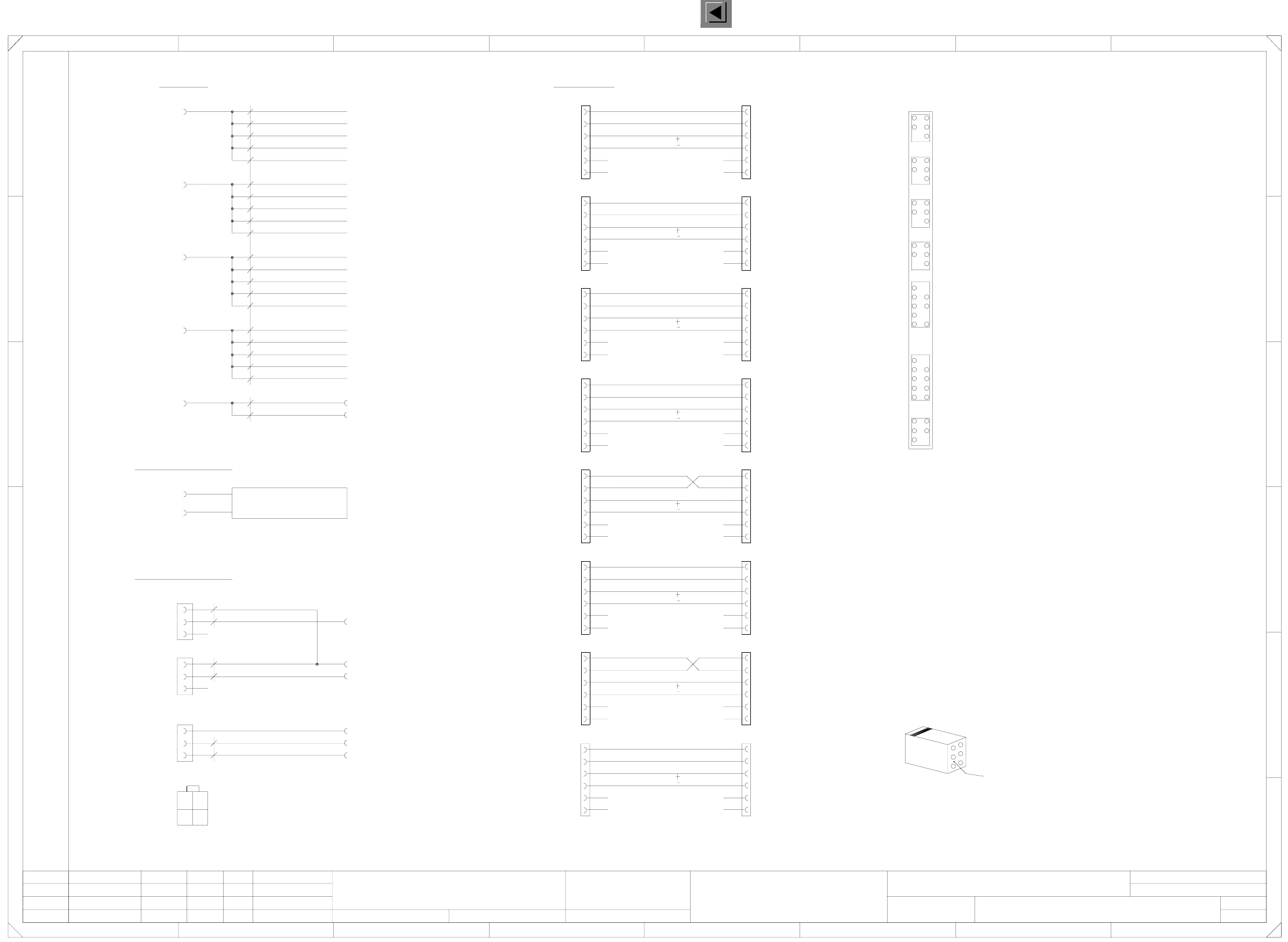
2 Circuit Diagr ams 85 I 0033589 1-010 202TD3 HS -50 servo unit without b oards , viewed f rom th e back (S h. 2 of 2) A3 HS50 servo unit, boards not instal led 2 (Viewed from the back) Potential distributor A44 (dp axis…
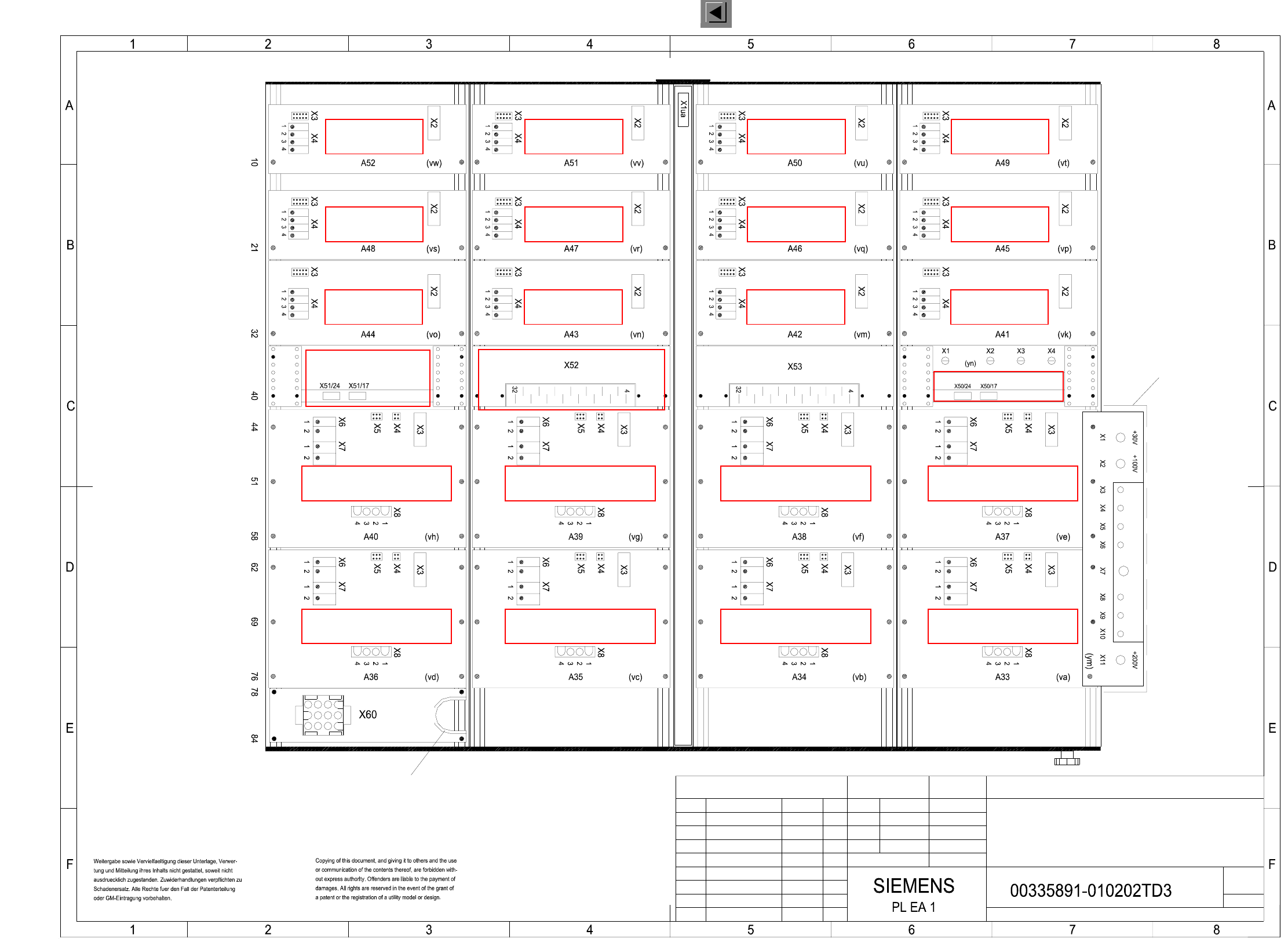
2 Circuit Diagrams 83
I
00335891-010201LD3 Servo unit without boards (Sh. 2 of 2)
Weitergabe sowie Vervielfaeltigung dieser Unterlage, Ver-
wertung und Mitteilung ihres Inhalts nicht gestattet, soweit
nicht ausdruecklich zugestanden. Alle Rechte vorbehalten, ins-
besondere fuer den Fall der Patenterteilung oder GM-Eintragung. Bauteilangaben nur zur Information
Comunicado como segredo empresarial. Reservados todos os direitos.
Confie a titre de secret d’entreprise. Tous droits reserves.
Proprietary data , company confidential . All rights reserved.
Confiado como secrete industrial. Nos reservamos todos los derechos.
SMD-Placement System Siplace HS50
Product status
Doc. status
Function status
Status DateModified Name Stand. Orig. Replacement for Replaced by
Author
Date
Check.
Sheet
Sh.
Tacho-X4
Enable
Tacho-Y4
Enable
Tacho-X2
Enable
Tacho-Y2
Enable
Tacho-X3
Enable
Tacho-Y3
S
Z
DP
X4vp/1
Key Key
b28 = Distance sensor, analog
Ventilation OK
X60/9
P24
a26 = Distance sensor, digital
Key Key
Key
Key Key
Key
Key Key
b21 = Distance sensor analog
b27 = B2-prox. switch Y4 [Y3]
a19 = Distance sensor, digital
1324567
Y
S
Z
DP
4 78
5
9
13
D
E
FF
Key
Key
Enable
Key
Key
Y
S
Z
DP
X4vs/1
X4vw/1
X52/24
bl / 0.34mm²
X-P1
X6va/1
X6ve/1
X4vk/1
Y
Y1 [Y2] - gantry
X4 [X3] - gantry
Y4 [Y3] - gantry
b
X51b7
X51a13
X51b13
b31 = 0 Volts
a31 = Crash signal
b32 = -15V
17
24
b17 = Ref. prox. switch X1 [X2]
b18 = B2-prox. switch X1 [X2]
Null
Key
Key
0.34mm²
X6vb/1
X6vf/1
X4vm/1
Y
S
Z
DP
X4vq/1
X4vu/1
X52/20
X-P2X6vc/1
X6vg/1
X4vn/1
X1ua/2
X1ua/1
X
X
X4vr/1
X4vv/1
X5va/3
C
B
A
X50a10
X50a9
X50b9
XX
X
XX
X
X50 [X51]
X1 [X2] - gantry
Gantry 1 [2]
Gantry 4 [3]
(Prox. switches)
(Prox. switches)
X=pinched off
1
30
X5vb/6
X5vc/2
X5vc/1
X5vc/4
a
a30 = Control On
b30 = +15V
X
X
X
65
b20 = B2-prox. switch Y1 [Y2]
b24 = Ref. prox. switch X4 [X3]
b25 = B2-prox. switch X4 [X3]
b26 = Ref. prox. switch Y4 [Y3]
X5vg/3
X5vg/6
X5vh/2
X5vh/1
X5vh/4
X5vh/3
X5vh/6
pk
vi
X60/6 Control On
bn
X1ua
bn
Crash signal P2/P3
X50a3
X50b3
X5va/2
X5va/1
X
E
D
X51a15
X51b15
X5vf/2
X5vf/6
X5vg/2
X5vg/1
X5vg/4
X51b1
X51a2
X51b2
X51a3
X51b3
X51a9
X51b9
X51a10
X51b10
X51a11
X51b11
X5vb/2
X5vb/1
X5vb/4
X5vb/3
X50/a32
X51/a30
X51/a31
X51/a32
X5vc/3
X
X
X5vd/1
X5vd/4
X5vd/3
X
X
X
X50a6
X50b6
X50a7
X50b7
0.34mm²
gn / 0.34mm²
0.5mm²
rd (UL)
bk (UL)
12
34
Viewed from
cable entry side
X50a1
X50b1
X50a2
X50b2
X50a5
X50b5
X52/22
X-P3
X5va/4
X51a14
X51b14
X6vd/1
X6vh/1
X4vo/1
X5vf/1
X5vf/4
X5vf/3
X50b10
X50a11
X50b11
X51a1
bl / 0.34mm²
Anticrash P1/P4X50/b32
X51/b32
X52/26
Anticrash P2/P3
-15 Volts
Ballast resistor
External
Ballast resistor
X53/10
X53/30
Anti-crash/fan
X50/a30
X50/a31
Tacho-X1
Anticrash
X60/8
X60/7
X60/5 Crash signal P1/P4
X60/10
X
X51a7
XX
X5ve/2
X5ve/1
X5ve/4
X5ve/3
X5ve/6
b19 = Ref. prox. switch Y1 [Y2]
X50a13
X50b13
X50a14
X50b14
X50a15
X50b15
X51a5
X51b5
X51a6
X51b6
X
X1ua/4
X5vc/6
X5vd/2
X5vd/6
2
Tek
Tek
Tek
1.
2.
1.
21.01.98
09.12.98
09.12.98
21.01.1998
Goller
#
Servo unit without boards
2
X
X4vt/1
X52/18
X-P4
X5va/6
00335891-010201LD3
PL EA1 E2
the numerical sequence of a Locking-clip connector
Make sure that ...
must be as viewed from the rear side of the casing.
Cable
=
SIEMENS AG
+
3
5
2
4
6
1
Enable
a21 = 0 Volts analog
Key Key
a28 = 0 Volts analog
8
123
Tacho-Y1
Enable
A
B
C
2 Circuit Diagrams 85
I
00335891-010202TD3 HS-50 servo unit without boards, viewed from the back (Sh. 2 of 2)
A3
HS50 servo unit, boards not installed
2
(Viewed from the back)
Potential distributor A44
(dp axis)
Backplane DC2,5
(Z axis)
(Star)
(Y axis)
Backplane AC12,5
(X axis)
Backplane AC12,5
(Y axis)
Backplane AC12,5
(X axis)
Backplane AC2,5
(Star)
Backplane DC2,5
(Z axis)
(dp axis)
Backplane DC2,5
(dp axis)
Backplane DC2,5
Backplane DC2,5
(Z axis)
Backplane AC2,5
(Star)
Backplane AC12,5
(Y axis)
Backplane AC12,5
(X axis)
Backplane AC12,5
(Y axis)
Backplane AC12,5
(X axis)
Backplane AC2,5
(Star)
(Z axis)
Backplane DC2,5
(dp axis)
Backplane DC2,5
Gantry IIGantry III Gantry IV Gantry I
Edge protection
potential distributor
Cover
0-Volt
02.
02.
Tek
Tek
Tek
26.01.99
07.12.98
01.12.97
Hoffmann01.12.1997
01.
1:2
2
Anticrash board X51
Power supply unit Ballast circuit
Anticrash board X50
Fan unit assembly A44
Backplane AC12,5
Backplane AC2,5
Backplane DC2,5
Function status
Product status
Doc. status
SMD Placement System SIPLACE HS50
FSUAUSESFS
26.01.99
Status Modified Date Name
Stand.
Check.
Author
Scale
Date
Name
(Drawing number)
Main no.
Sheet
Sh.
See page 151
See page 140
See page 140
See page 149
See page 150
See page 150