Specification SIPLACE CA-Series2014版.pdf - 第6页
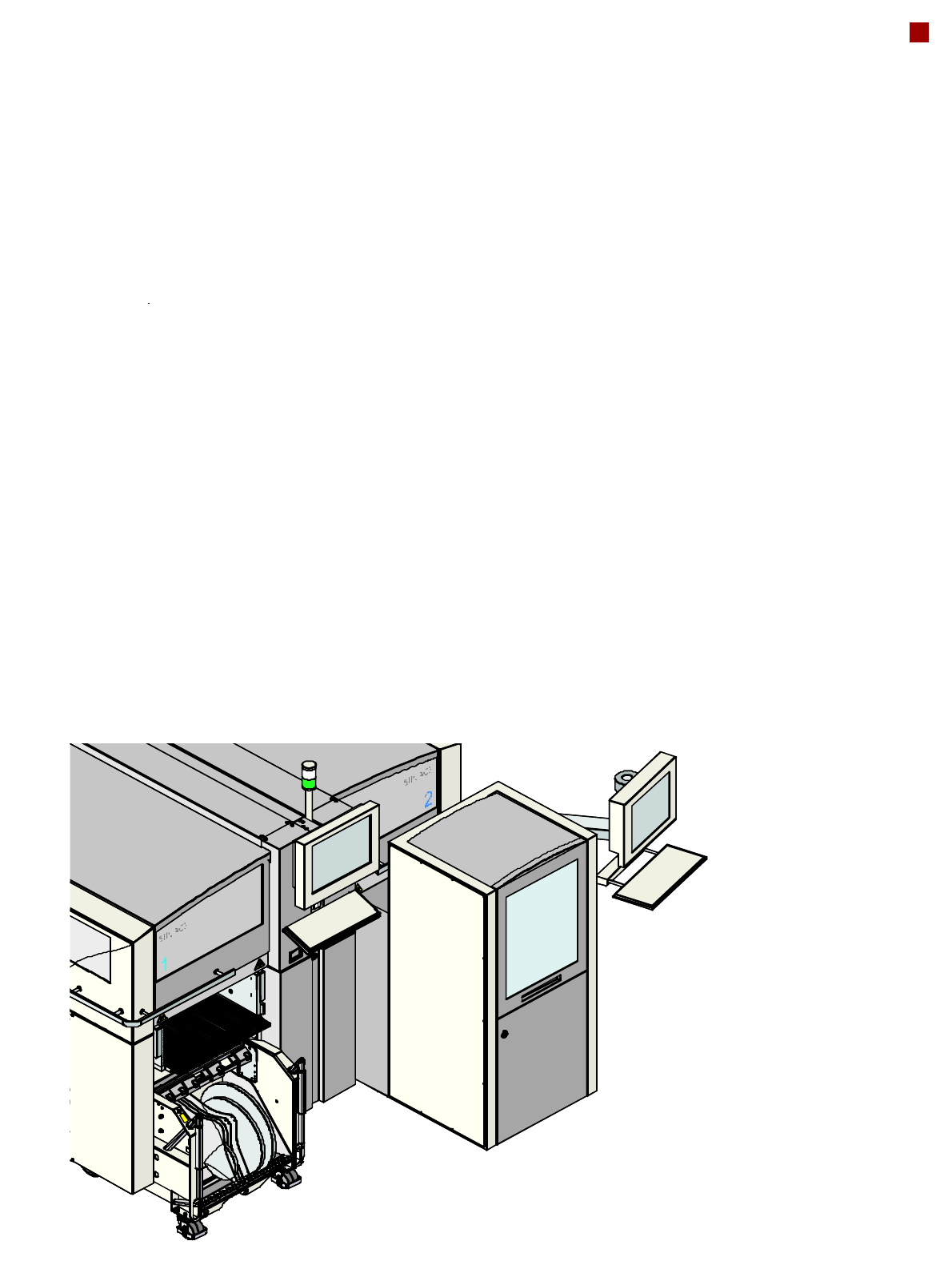
6 Machine Description Overview General The SIPLACE CA (Chip As- sembly) platf orm can place bare dies d irectly from the wafer, using the die attach or flip chip process. Th is pro- vides additional support for the SMT p…

5
Overview of Technical Data
Maximum Values
Pickup on SWS Pickup on
X-table
Flip Chip Die Attach SMD
Accuracy
a
C&P20 M
CPP
TH
a) 10µm at 3σ in placement process with the "Embedded Wafer Level Ballgrid Array" option (on request).
± 10 µm at 3σ
± 25 µm at 3σ
--
± 10 µm at 3σ
± 25µm at 3σ
--
± 20 µm at 3σ
± 25 µm at 3σ
± 22 µm at 3σ
b
b) With stationary camera, type 25
Placement performance
c
c) The placement performance depends on several project-specific parameters. The ex-
pected throughput can be individually calculated on request.
4 SWS, without dipping 4 SWS SMD
C&P20 M
CPP
TH
42,000 die/h
42,000 die/h
--
28,000 die/h
26,000 die/h
--
See page 8
Die / component size
Flip Chip Die Attach SMD
C&P20 M
CPP
TH
0.5 x 0.5 mm
d
e
to 6 x 6 mm
0.5 x 0.5 mm
d e
to 27 x 27 mm
--
d) Smaller dies on request
e) Dipping: depends on process
0.8 x 0.8 mm
d
to 6 x 6 mm
0.8 x 0.8 mm
d
to 27 x 27 mm
--
See page 14
See page 15
See page 17
Feeder module
types
Tape feeder module, waffle pack tray, stick magazine
feeders, bulk case, dip module, application-specific
OEM feeder modules, SIPLACE Wafer Feeder (SWS)
Supply capacity
(Component trolley
SIPLACE X)
160 tape feeder modules 8 mm X
Substrate size 50 mm x 50 mm to 535 mm x 850 mm
f
f) 850 mm on request
Substrate thickness 0.3 mm to 4.5 mm

6
Machine Description
Overview
General
The SIPLACE CA (Chip As-
sembly) platform can place
bare dies directly from the
wafer, using the die attach or
flip chip process. This pro-
vides additional support for
the SMT placement options
available with SIPLACE X
series machines. The
SIPLACE CA can either be
used only for bare die or SMT
placement or in single pass
mode. In this case, both bare
dies and SMT components
can be placed during the
same process. Users benefit
from a combination of great-
er process flexibility and
higher placement speeds
which is unique to the elec-
tronics production industry.
The SIPLACE CA-Series is
available with 4 gantries.
The SIPLACE CA4 can be
configured with up to 4 SWSs
(S
IPLACE Wafer System).
The SWS provides the place-
ment head with components
(dies) directly from the wafer
(max. 12“).
Placement Machine
The placement machine
uses the Collect&Place
method for high-speed
placement of standard com-
ponents.
The moving head picks the
components up from the
waiting SWS and places
them on the waiting printed
circuit board. This proven
SIPLACE principle has many
advantages:
• No downtime due to refill-
ing or splicing
• Reliable pickup of even
the smallest components
• No shifting of the compo-
nents on the circuit board
• Minimized travel range
High flexibility, economic effi-
ciency and reliable setups
are the guarantee for the
high level of productivity in
the SIPLACE CA series
placement systems.
Minimum down times
increase utilization and thus
help to increase productivity.
Even the very small 03015/
01005 components can be
processed with the
SIPLACE CA-Series.
SIPLACE Wafer System
SWS
The integration of the
SIPLACE Wafer Systems
(SWS) in the SIPLACE CA
enables you to place dies
directly from the wafer, using
the standard SMT placement
procedure. This unique
placement platform supports
both the flip chip and the die
attach process.
• Processes supported:
Flip chip, die attach (chip
on board), SMT
• Hoopring handling
• Horizontal wafer system
• Automatic wafer change
• Linear Dipping Unit
• Die attach unit
• Wafer map connection
(e.g. ALPS)
• Multi-die capability
7
Machine Description
SIPLACE Wafer System
Description
The SIPLACE Wafer System
(SWS) makes the compo-
nents available to the place-
ment head, directly from the
wafer. The SWS therefore
extends the component
spectrum of the established
SIPLACE X machines, by
enabling placement of bare
dies from wafers.
The wafers are supplied fully
automatically out of the wafer
cassette and the dies inside
can be processed in the
established placement pro-
cedures.
Flip chip process - func-
tion
The wafer is fully automati-
cally pulled out of the wafer
cassette and is then trans-
ported to the wafer table. The
wafer table positions the die
above the ejection system
that releases the die from the
wafer foil. After this release
procedure, the flip unit noz-
zle takes the die, rotates it by
180° and makes it available
to the placement head for
pickup.
Options
The process spectrum is
supplemented by the follow-
ing options:
– Die attach unit:
The die attach unit takes
the die from the flip unit
nozzle and turns it, so that
it has the same top-bottom
orientation on the board
as it had on the wafer.
– Linear Dipping Unit
The Linear Dipping Unit
distributes precise layers
of flux for the flip chip pro-
cess. After taking over
from the flip unit, the
placement head dips the
die into the flux layer.