20121120111955_KY8030_2_Maintenance_Manual_Eng_ver1.pdf - 第54页
54 | KY -8030 2 3D Solder Paste Inspec tion System V ersion 1.0 K OH Y OUNG T ECHNOLOGY I NC . 1.2.16.6. Electric Box Cleaning Figure 1-22. Electric Box 1. Cut the power/the air supply and press e…
Maintenance Manual | 53
5. Supplypowerandcheckifthesystemisoperatingproperly.
Note:Becarefulforthehazardofelectricshock.
54 | KY-8030 2
3DSolderPasteInspectionSystem
Version 1.0
KOH YOUNG TECHNOLOGY INC.
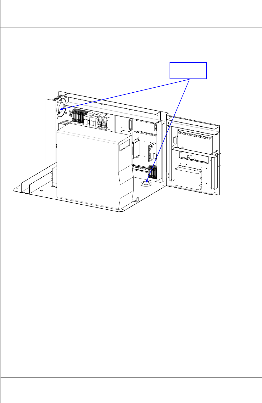
1.2.16.6. Electric Box Cleaning
Figure 1-22. Electric Box
1. Cutthepower/theairsupplyandpressemergencyswitch.
2. OpentheFrontDoor/WindowanddisassembleRearCover/RightSideCover.
3. OpenalltheDoorsofElectricBoxatthelowerpartofthesystem.
4. EliminatedustintheElectricBoxwithcompressedairandvacuumcleaner.
5. Check
theConnectorstate.
6. Supplypowerandcheckifthesystemisoperatingproperly.
Cleaning
Spot
Maintenance Manual | 55
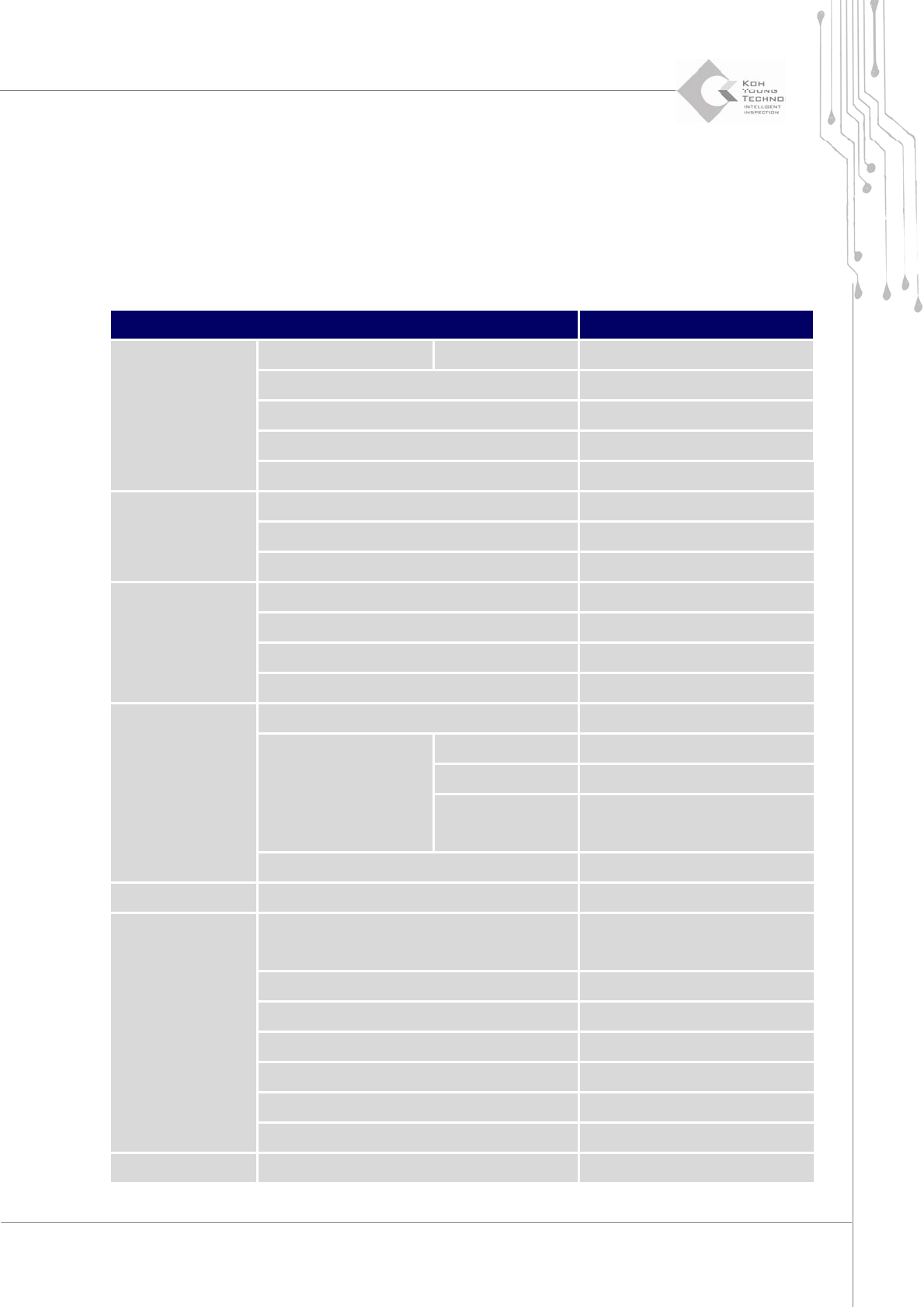
2. APPENDIX
2.1. Main Features of the System
2.1.1. SYSTEM SPECIFICATIONS: KY-8030 2
Classification KY-8030 2
Inspection
Performance
Inspection Speed Dual Mode 30cm2/sec
FOV(Field of View) 47.0x34.6mm
Solder Paste Height Range
40~600㎛
XY Pixel Resolution (㎛) 20㎛
Height Resolution [microns]
0.37㎛
XY Robot
Moving Speed 1m/sec
Resolution
1㎛/pulse
Accuracy
±20㎛
Installation
Requirement
Electrical supply 200-240VAC, 50/60Hz
Power Consumption 10amps (RMS peak)
Compressed Air
5Kgf/㎠
Air Consumption 50NI/min(1.8cfm)
System
Type & Direction Front Fix, Left → Right
Dimension
Width 1000mm
Depth 1203mm
Height
1570mm(PCB Transfer Height
950mm)
Weight 550kg
Sound Noise dB Lower than 73
PCB Specification
Working Area
Max. 510x510mm
Min. 50x50mm
PCB Thickness 0.4-4.0mm
Load Height 870~970mm
Max. PCB Weight 2kg
Edge Side Clearance Top 2.5mm
Edge Side Clearance Bottom 3.5mm
Bottom Clearance 30mm
Control Unit Control Method PC Based Control (Windows)