ENG_SS_108-90801_E.pdf - 第3页
Product specification ‘ Multisprin g standard power ’ 108 - 90801 ..........................................................................................................................................................…
Product specification ‘Multispring standard power’ 108-90801
................................................................................................................................................................................................................................................…………………..
Rev. E Page 2 of 7
R1-1 (Rev. 02-00)
1. SCOPE .
This specification covers all the information as required in the IEC 60352-5 (Issue 5; Jan 2012) for a
Multispring Press-In zone (further named “Multispring”) for nominal hole-Ø 1.45mm and made from
0.8mm stock thickness.
The IEC requirements are supplemented with the requirements for automotive use (in the engine area)
based on the “Arbeitskreis Prüfrichtlinie für KFZ-Steckverbinder“.
2. PRINTED BOARD AND HOLE INFORMATION
Printed board material according to :
IEC 61249-2-7 (replacement for the IEC 60249-2-4/5/11/12)
Other board materials are possible and have to be tested on request.
Maximum number of conductive layers: not limited.
Printed board thickness:
Normal range: min = 1.6mm ±0.14 mm; max = not limited.
Extended range: Min = 1.2mm … max = 1.6mm: allowed with some restrictions:
* The maximum deformation of the PCB-hole according to the IEC-norm cannot be
guaranteed for all types of PCB material used.
* With some plating combinations the hold force can be smaller than the limit of min.40N.
* Electrically less current can be put thru the press-fit and should be checked
* An application test is necessary to test the project specific situation
Smaller board thicknesses have to be tested.
Plated-Through-Hole dimensions:
Hole-Ø prior to plating = 1.6±0.025 mm
Thickness of the PTH-wall > 25 µm Cu
Finished hole-Ø = 1.45-1.54mm
in case of HAL PCB’s or exceptional cases the former standard of 1.39-1.54mm is allowed.
Printed board plating material :
HAL or galvanic tin plated 5 –15 µm
Chemical Sn > 0.5µm
0.05-0.2µm Au over 2.5-5 µm Ni
OSP (Organic Solderability Preservative) (not recommended)
Other plating materials have to be tested on request.
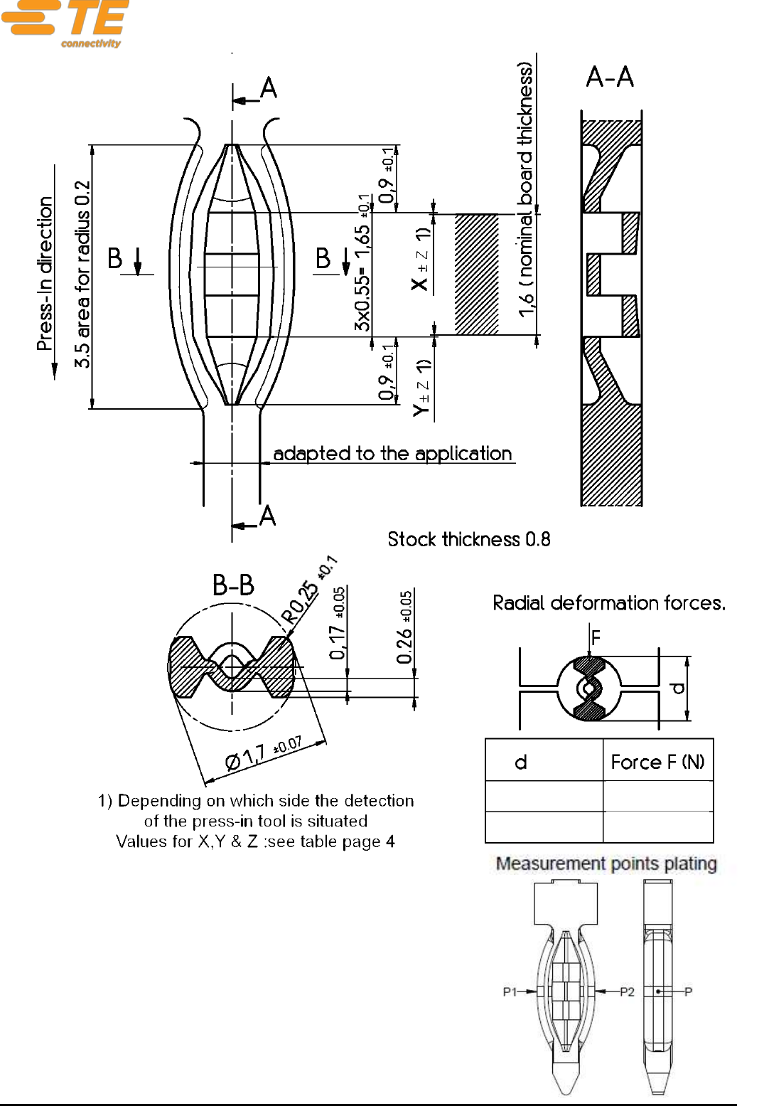
3. PRESS-IN ZONE INFORMATION
Design : see dimensional drawing on page 3
Material : CuSn4 , CuSn6 ,CuNiSi or CuCrAgFeTiSi or similar copper alloy.
Other materials have to be tested on request.
Plating : - 0.4-1.5 µm Sn over min 0.8µm Ni.
- 0.4-1.5 µm SnPb over min 0.8µm Ni. (Technically possible but decommissioned)
- 0.3-1.1 µm S+D Advanced Indium over 1.27…2.2 µm Ni.
- Customer specific plating definitions are possible but have to be tested.
Not all combinations of plating, base material and PCB plating/technology are possible or
released. In case of doubt, please contact TE.
Product specification ‘Multispring standard power’ 108-90801
................................................................................................................................................................................................................................................…………………..
Rev. E Page 3 of 7
R1-1 (Rev. 02-00)
1.42
1.57
min 110
max 300
Product specification ‘Multispring standard power’ 108-90801
................................................................................................................................................................................................................................................…………………..
Rev. E Page 4 of 7
R1-1 (Rev. 02-00)
4. INFORMATION ON THE APPLICATION.
The Multispring as described can be used as a
Individual press-in termination.
Straight or right angle termination.
Rear plug up.
Wrapped connection.
Connector or module with pre-assembled press-in terminations.
5. INSTRUCTION AND TOOLS FOR THE PRESS-IN OPERATION.
Depending on plating combination minimum 1 replacement is guaranteed with a new press-in
termination.
More repairs have to be tested on request.
Press-in depth :
As on the dimensional drawing on page 3 for the minimum thickness printed board.
For thinner printed boards the position of the printed board should be situated in the middle of the
press-in zone. Notice that some press-fit parameters can be affected and have a lower performance
(e.g. Retention force) see also paragraph 2: ‘PCB definition’. In case of PCB’s with a smaller
thickness of 1.6mm nominal, a project specific test is recommended.
For thicker printed boards the position of the press-in zone should be preferably
in the middle or in the upper half of the printed board thickness. See the application drawing and
table.
For complex geometry with a high number of pins, the dimension of X±0.2mm can be interpreted of
the mean of all press-in depths. The maximum single press-in depth should however been within
Y±0.3mm.
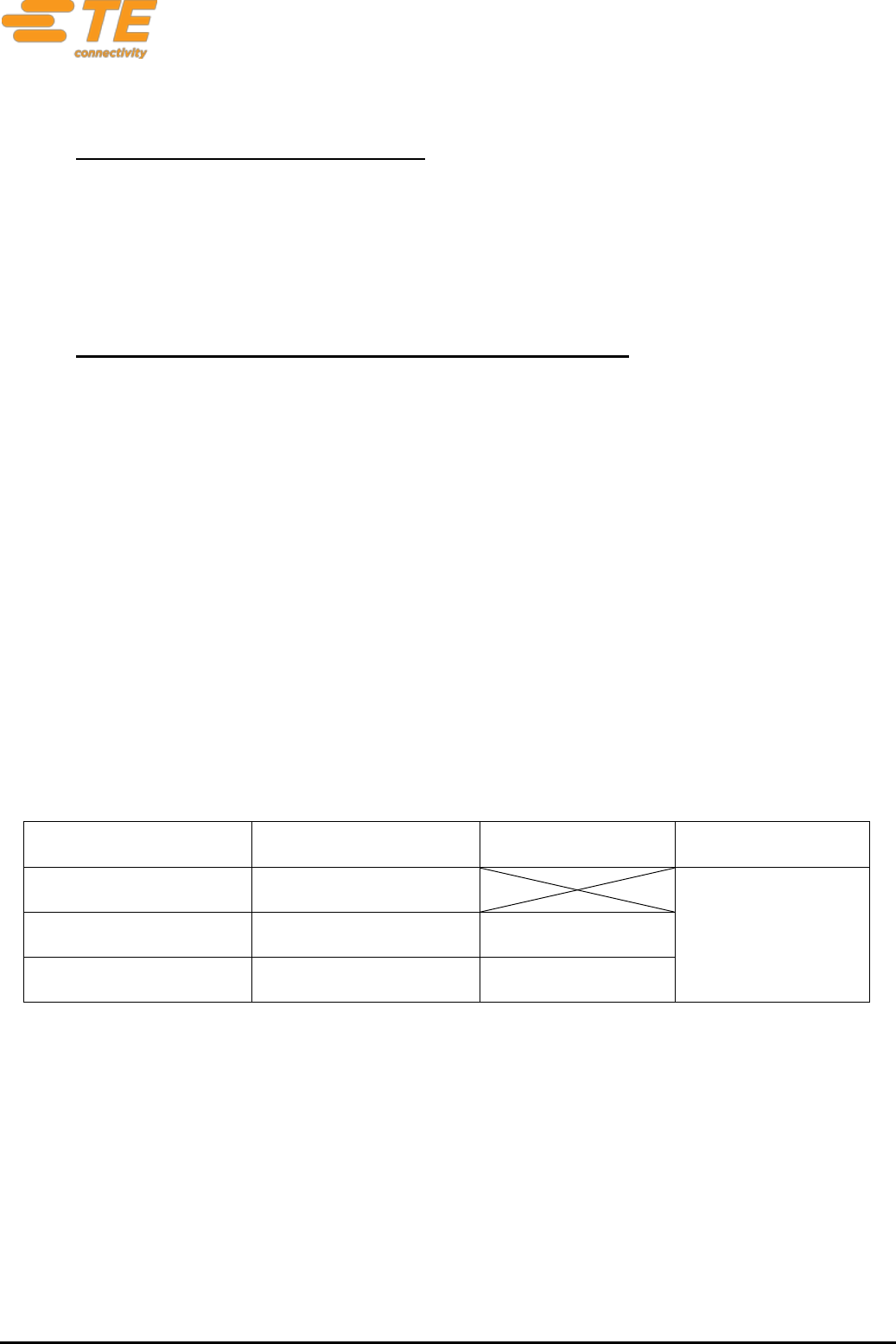
PCB Thickness
Nominal Press-in
dimension X
Nominal Press-in
dimension Y
Tolerance Press-in
dimension Z
> 1.6 mm
0
0.2 (0.3 *)
1.6 mm
0
0
1.2…1.6 mm
0.1 - k
0.1 – k
With k = (1.6 – PCB Thickness) / 2
*) For complex applications with a high number of pins, the tolerance Z of ±0.2 mm can be extended
towards ±0.3 mm. The mean of all press-in dimensions of the application should however still lay
within the ±0.2 tolerance range.
For standalone pins as Single Pin Insertion, the depth tolerance of
+0.2 mm to -0.2 mm is mandatory.
The use of the middle of the Multispring as reference for press-in depth will be less accurate and is
not recommended. One should choose between dimension X or Y to define the right press-in depth
dimension. This choice of reference is determined by the application (housing, module, stand-alone
pin…) and the used press-in tooling (detection, reference side of the PCB,…). In that way the usual
big tolerances of the PCB thickness can be avoided to optimize the press-in process and the
tolerance calculation chain.