OM-1650-001_w.pdf - 第23页
OM-1650 20 9. Bad Mark Camera T est PEC Recog [Continuation] Button : When selected, the recognition test is performed continuously. [Step] Button : When selected, the recognition test is performed step by step. [Set to …
OM-1650
19
9. Bad Mark Camera Test
9. Bad Mark Camera Test
When the camera system is used in the bad mark detection function, the
"Threshold" is calculated to set the "Value of threshold" on the "PCB Data" sub-
tab sheet on the "Operation Data" tab sheet.
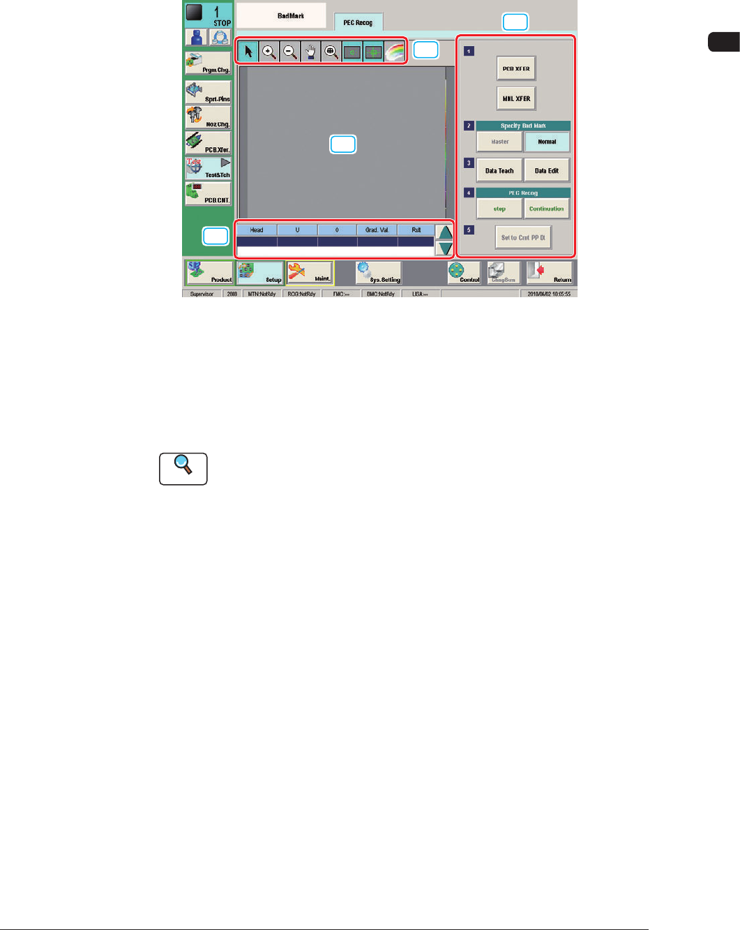
[1]
[3]
[2]
[4]
F14
[1] Displayed Image Operation Button
Using the following buttons, the modes for performing the enlarging or
movement operation for the image displayed in the recognition image display
pane [2], are changed.
Reference
Refer to "7. Test and Teaching" in Chapter 6 in Volume 2 in the
SIGMA-G4/G5 Instruction Manual for the displayed image operation
buttons.
[2] Recognition Image Display Section
The recognition results are displayed in this section.
[3] Bad Mark Camera Test Measurement Results
The bad mark camera test measurement results are displayed in this section.
[4] Operation Buttons
Specify Bad Mark
[Master] Button
: This button is selected when the Master Bad
Mark Detection (Overall BBR Detection) is to be
performed.
[Normal] Button
: This button is selected when the normal BBR
detection (individual detection) is to be performed.
[Data Teach] Button
: This button is selected when the data teaching is to
be performed.
[Data Edit] Button
: This button is selected when the data editing is
performed.
1006-001
OM-1650
20
9. Bad Mark Camera Test
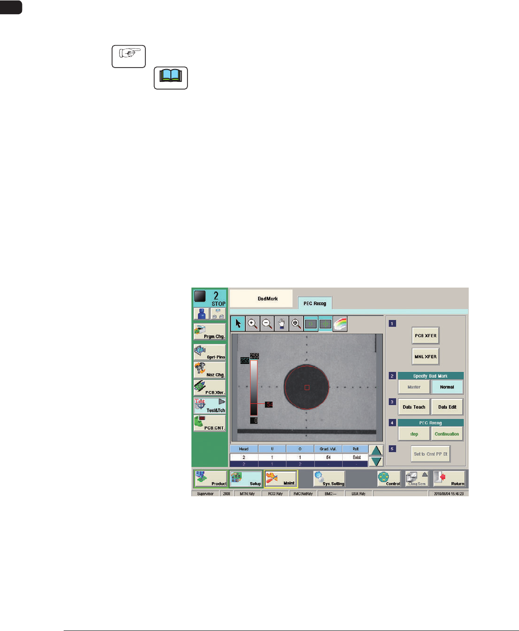
PEC Recog
[Continuation] Button
: When selected, the recognition test is
performed continuously.
[Step] Button
: When selected, the recognition test is
performed step by step.
[Set to Cmt PP Dt] Button
: When selected, the test data after data editing
is registered as the pattern program data.
Judgement Threshold Calculation Procedure
Procedure
(1) Put a bad mark on the PCB to be produced.
Note
(a) Use a black mark as a bad mark for a comparatively bright PCB detection
area (PCB with a lot of light reflex).
Use a white mark as a bad mark for a comparatively dark PCB detection
area (PCB with a little light reflex).
(b) When the selection is changed (from "Black Mark" to "White Mark" or
vice versa), be sure to change the mark image ("Black (E/NR)" or "White
(E/R)" in the related "Mark Image" text box of the pattern program data.
(2) Move the PCB to be produced to the PCB positioning section.
(Transfer the PCB to the block where the bad mark is detected using the PEC
recognition camera, using the [PCB XFER] button or [MNL XFER] button).
(3) At first, select the unit PCB with a bad mark and perform the "Step Move".
Then, select the unit PCB without a bad mark and perform the "Step Move".
Bad Mark Exist F15
1006-001
OM-1650
21
9. Bad Mark Camera Test
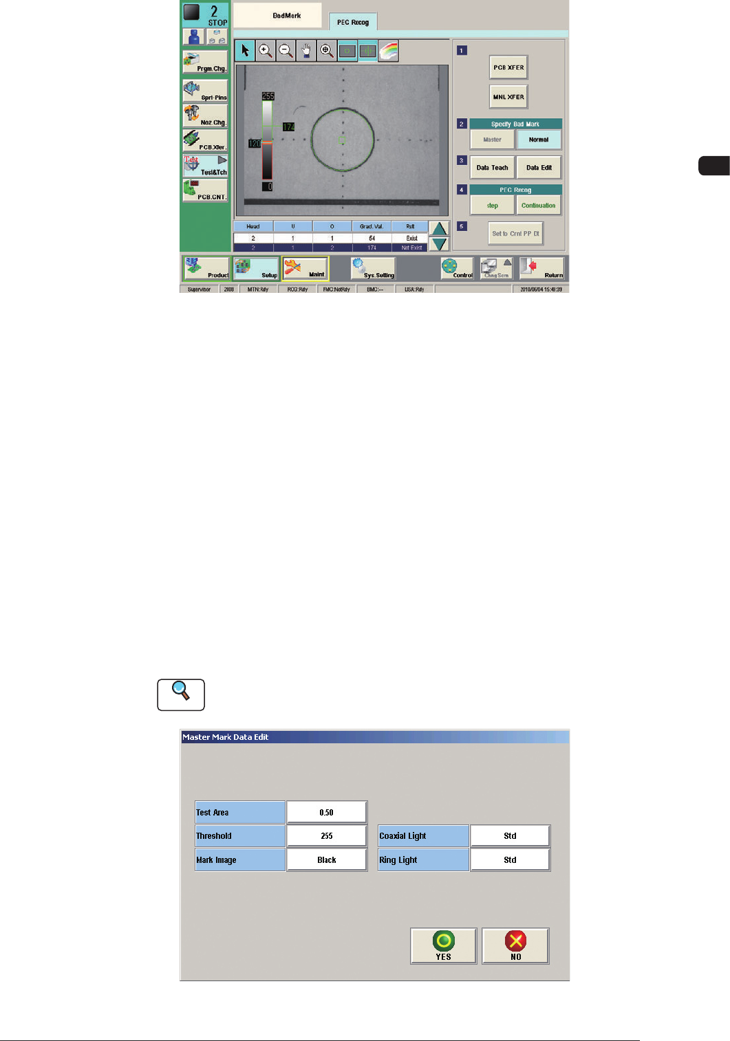
Bad Mark Not Exist F16
As a result of the camera test and measurement for bad mark detection, the
gray value of the bad mark is indicated in the "Grad.
Val." cells and "Exist" or "Not Exist" in the "Judge" cells.
The mean value of the gray values for "Exist" and "Not Exist" (Bad Mark
Detection) is regarded as a threshold value for the bad mark detection.
Example :
Result of Measurement
85 in "Grad. Val." Cell for "Exist" in "Judge" Cell
199 in "Grad. Val." Cell for "Not Exist" in "Judge" Cell
85 + 199 = 284 ÷ 2 = 142 = Threshold Value
(4) When the data is to be taught, press the [Data Teach] button and when the
data is to be edited, press the [Data Edit] button.
Reference
When the data teaching is to be performed, refer to "10. Camera Bad Mark
Teaching".
Specify Bad Mark : Master F17
1006-001