NYT-M2_DS_2020v1F.pdf
Aut oma t ed Op tic al Inspection f or Adv anc ed Micro Elec tronics www .nordson.c om YES TECH M2
Automated Optical Inspection for
Advanced Micro Electronics
www.nordson.com
YESTECH M2
2 | YESTECH M2 Micro Electronics Inspection 3 | YESTECH M2 Micro Electronics Inspection
O
v
e
r
m
o
l
d
W
a
f
e
r
R
e
c
o
n
s
t
i
t
u
t
i
o
n
B
u
m
p
i
n
g
D
i
e
S
t
a
c
k
i
n
g
D
i
e
A
t
t
a
c
h
The Electronics People
Surface
preparation
Underll
Conductive
paste apply
Wire bond
inspection
Bond voiding
Die placement
Wire bond
inspection
Bump
metrology
Die adhesion
testing
Bond test
Bonded wafer
delamination
Package
delamination
Via cleaning
WLP underll
Bump and via
metrology
Stacked die
attach
Surface
preparation
Surface
preparation
Surface
preparation
Surface
preparation
Bond voiding
Die placement
Wire bond
inspection
W
i
r
e
B
o
n
d
Founded in 1954, Nordson Corporation is a
market leading industrial technology company
with annual revenues of over $2 billion and
more than 7,500 employees worldwide.
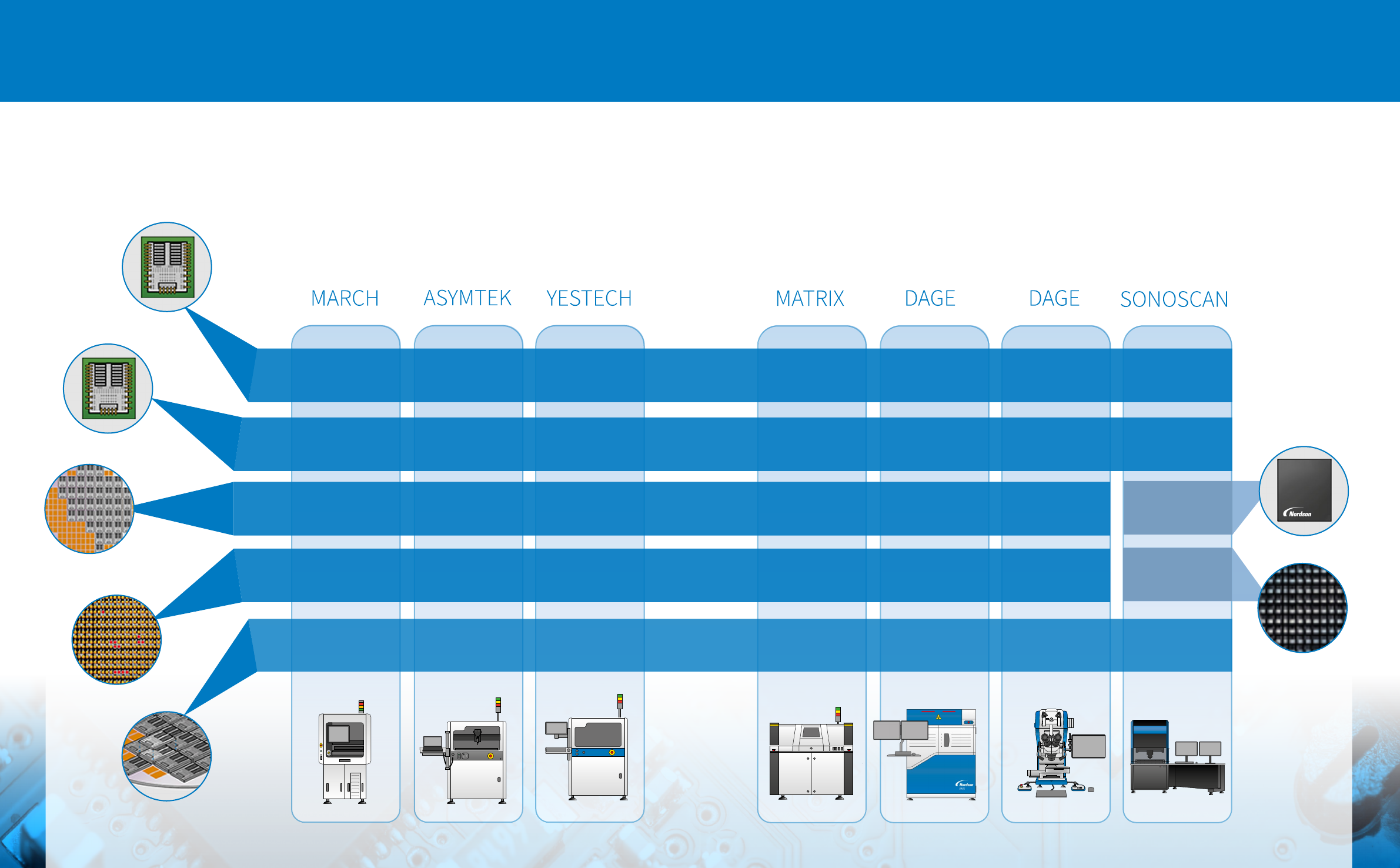
Nordson oers a wide range of products which are focused on providing process, test and inspection
solutions for the electronics and semiconductor industry. Whether you need to prepare a PCB using
MARCH plasma treatment technology, or check for package level delamination with SONOSCAN acoustic
inspection, we provide best in class technology solutions for PCBA and package level electronics
manufacture, and the global support network to keep you running and minimize downtime.
Bump
metrology
Die inspection
Underll llet
inspection
Die placement
contamination
4 | YESTECH M2 Micro Electronics Inspection 5 | YESTECH M2 Micro Electronics Inspection
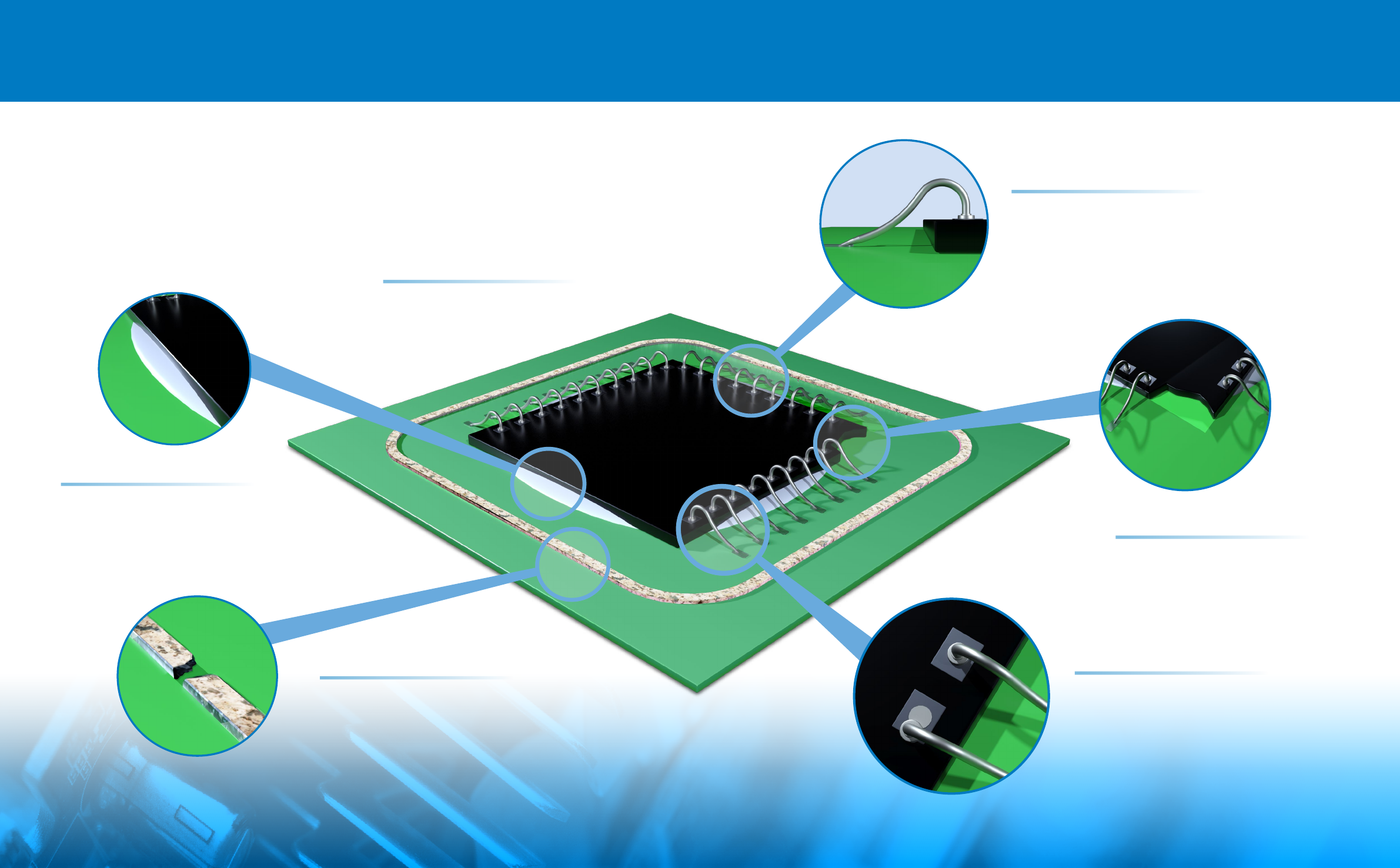
Wire bond height
Wire bonds which do not follow the design path can cause
bridging, opens, or may not be adequately encapsulated.
Optical metrology measures bond height and wire sweep
which are great quality indicators.
Problems Solved
Underll
Too little underll can lead to poor adhesion,
too much can lead to contamination. Inspect
underll to ensure within limits.
Ever increasing requirements for durability and reliability, along with a continuous drive to smaller
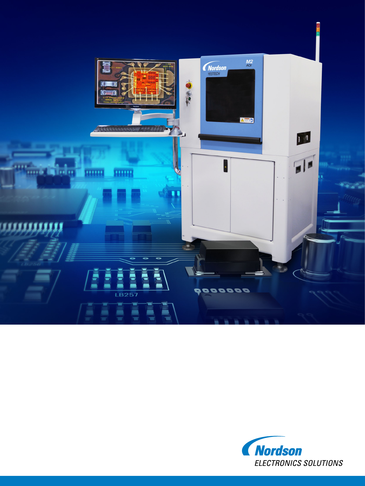
components means that ensuring quality product manufacture is now more important than ever.
M2 automated optical inspection ensures product quality is maximised. Reduce costly returns
from the eld and the associated damage to reputation and future business.
Bond quality
The position of the wire bond conrms
good on pad location, and can also indicate
process dri. The shape of wire bonds indicates
the bond quality. Inspect both with AOI.
SPI
Solder paste or epoxy is oen applied
as part of the encapsulation process.
Inspect position and quantity of paste
to ensure good encapsulation reow.
Chip outs and cracks
Can signicantly aect
device performance.
Contamination
Contaminated dies can suer functional and
lifetime issues. Foreign object detection
screens for contamination.