A10011-ASM-T53-EN-Spec-TX-micron-DMS.pdf - 第22页
22 SIPLACE Vision OnBoard Inspection and Pattern Matching OnBoard Inspection The OnBoard PCB Inspec- tion (SW option) uses the PCB camera to inspect criti- cal areas of the board, spec- ified by the user, e.g. under BGA …
21
Component feeding
Alternative SIPLACE feeder modules
JTF-ML 2
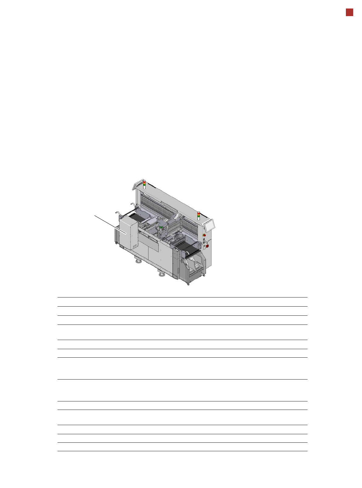
The SIPLACE TX micron
can accommodate a
SIPLACE JTF-ML 2 at
location 1. The SIPLACE
JTF-ML 2 is fitted to the side.
Depending on the magazine
type, the SIPLACE JTF-ML
2 stores up to 18 thin or, as
an option, 14 thick JEDEC
waffle pack trays in an
exchangeable cassette and
supplies them as required.
The placement machine can
therefore be supplied with
different component types at
variable waffle pack tray
changeover times.
An output conveyor
extension is required when
using the JTF-ML 2. This
extends the conveyor by
600 mm.
Technical data
Width x length x height (tower)
374.5 mm x 322.7 mm x 707.0 mm
Width x length x height (conveyor)
356.2 mm x 346.0 mm x 68.2 mm
Weight
Tower (empty): 26.3 kg (58.0 lbs.)
Total: ~36 kg (79.4 lbs.) (depending on application)
Storage capacity
JEDEC waffle pack tray specification JEDEC Standard: 95-1 & IEC 60286-5
Waffle pack tray, thin 18 JEDEC waffle pack trays or
18 magazine trays (cookie trays)
(in two cassettes)
Thick waffle pack tray 14 JEDEC waffle pack trays or
14 magazine trays (cookie trays)
(in two cassettes)
Waffle pack tray changeover time 3.15 to 6.1 seconds (depending on application
a
)
a) 3.15 seconds to the next waffle pack tray with maximum acceleration, 6.1 seconds from the first to the
ninth waffle pack tray with minimum acceleration.
Slot n to n+1 3.15 to 5.4 seconds (maximum/minimum accelera-
tion)
Cassette
Width x length x height 343.7 mm x 136 mm x 137 mm
Max. load weight (per cassette 4.45 kg (incl. weight of cassette)
JTF-ML 2
22
SIPLACE Vision
OnBoard Inspection and Pattern Matching
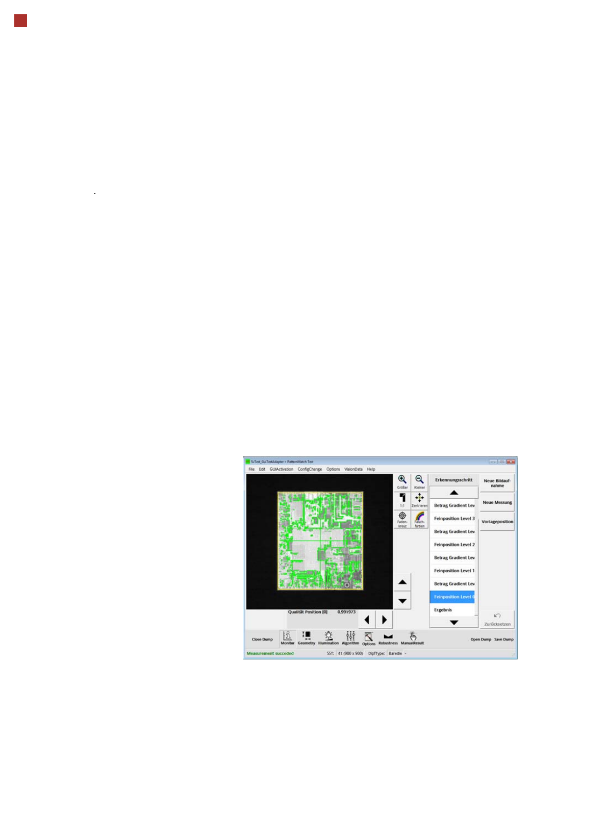
OnBoard Inspection
The OnBoard PCB Inspec-
tion (SW option) uses the
PCB camera to inspect criti-
cal areas of the board, spec-
ified by the user, e.g. under
BGA or shields just before or
after placement, to make
sure that all components
were placed or to make sure
that there are no objects in
the way of the placement
process.
It is also possible to inspect
the solder paste to make
sure that it is present. How-
ever, this must always be
performed at the first place-
ment machine, before place-
ment begins.
A requirement for all inspec-
tion tasks is that a "good pat-
tern" has been saved before
starting.
Pattern Matching
Pattern matching can be
used for components with
very fine contact pads, which
can not be detected with the
existing component camera
resolution. Searching and
detection is performed over a
larger area, which contains
unique structures (patterns).
Once the specified area has
been detected, the compo-
nent is aligned and placed
according to the position of
this area and in relation to the
substrate.
23
SIPLACE Vision
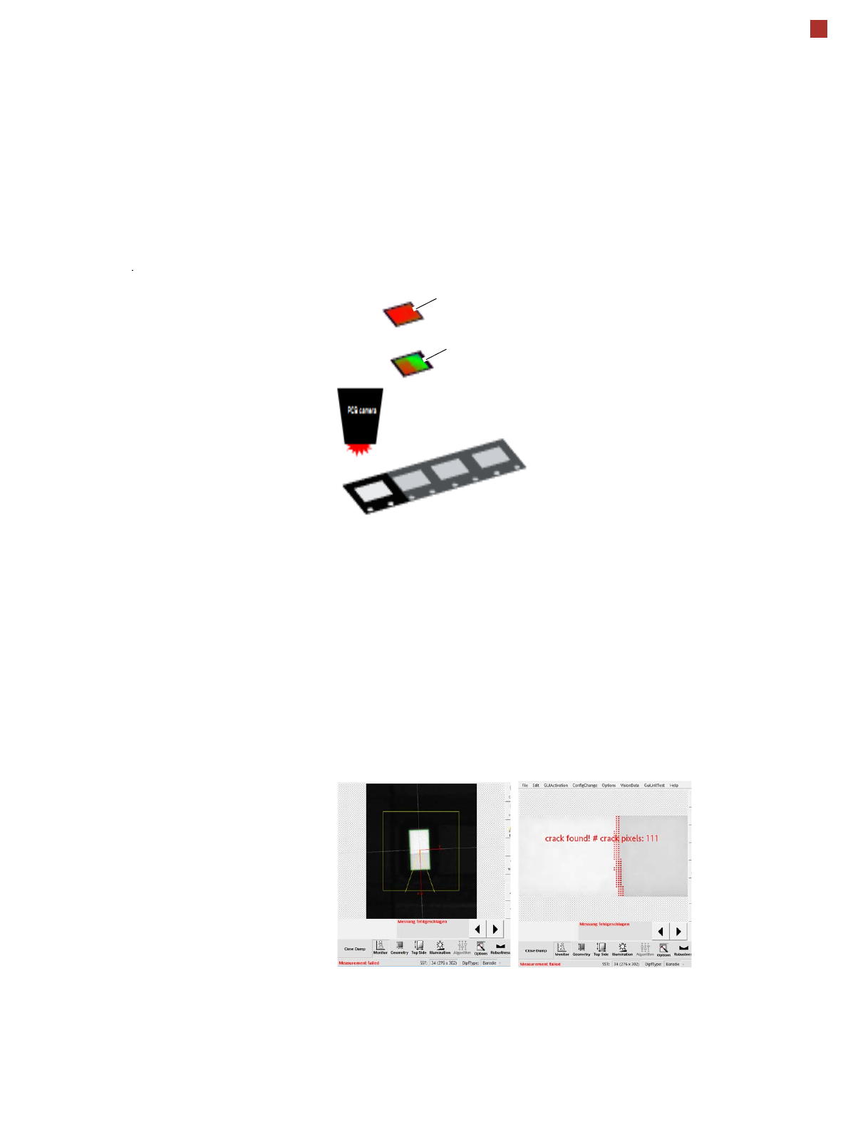
Cracked Die and Chipping Inspection
Crack Die Detection
The cracked die inspection
can detect breaks before
removal from the tape, if the
crack runs between two
outer edges of the die.
Inspection is performed
with the PCB camera. A
prerequisite for detection is
that the two parts of the die
are slightly inclined towards
one another. Detection is
possible via the differing
reflection angles of the two
surfaces which are inclined
towards one another.
Chipping Detection
Chipping detection allows
you to recognize chipped
areas on semiconductor
components.
Good
Bad