KE-750_QA表.pdf - 第81页
FUNCTION NAME 0.4 VCS, 0.3 VCS Light M ap Function/Performance CHECK/ADJUSTMENT METHODS (REMEDIAL ACT ION PROCEDURE) ASSURED QUALITY Reliability QUALITY CHARACTERISTI CS (SPECIFIC ATION VALUES) CATEGORY Safety Product Im…
FUNCTION NAME OCC Light R Histogram Function/Performance CHECK/ADJUSTMENT METHODS (REMEDIAL ACTION PROCEDURE)
ASSURED QUALITY Reliability
QUALITY CHARACTERISTICS (SPECIFICATION VALUES) CATEGORY Safety
Product Image
ROLE IN FUNCTION (MEANING OF SPECIFICATION VALUES)
POSSIBLE MALFUNCTIONS (CAUSED BY INCORRECT SPECIFICATION VALUES)
COMPONENTS
NO. Part No. Part Name Associated Quality Characteristics
1 E86067250A0 Base unit board assembly DC power source output voltage adjustment
2 E86247150A0 BOC light board assembly
3 MODEL KE-750/760
4 UNIT Electrical REF. NO.
5
NAME
EL-10
6 FUNCTION OCC Light R Histogram
7
NAME
8
9
10
QA Table
1. Before making the adjustment, make sure that the DC power source output voltage has been properly adjusted.
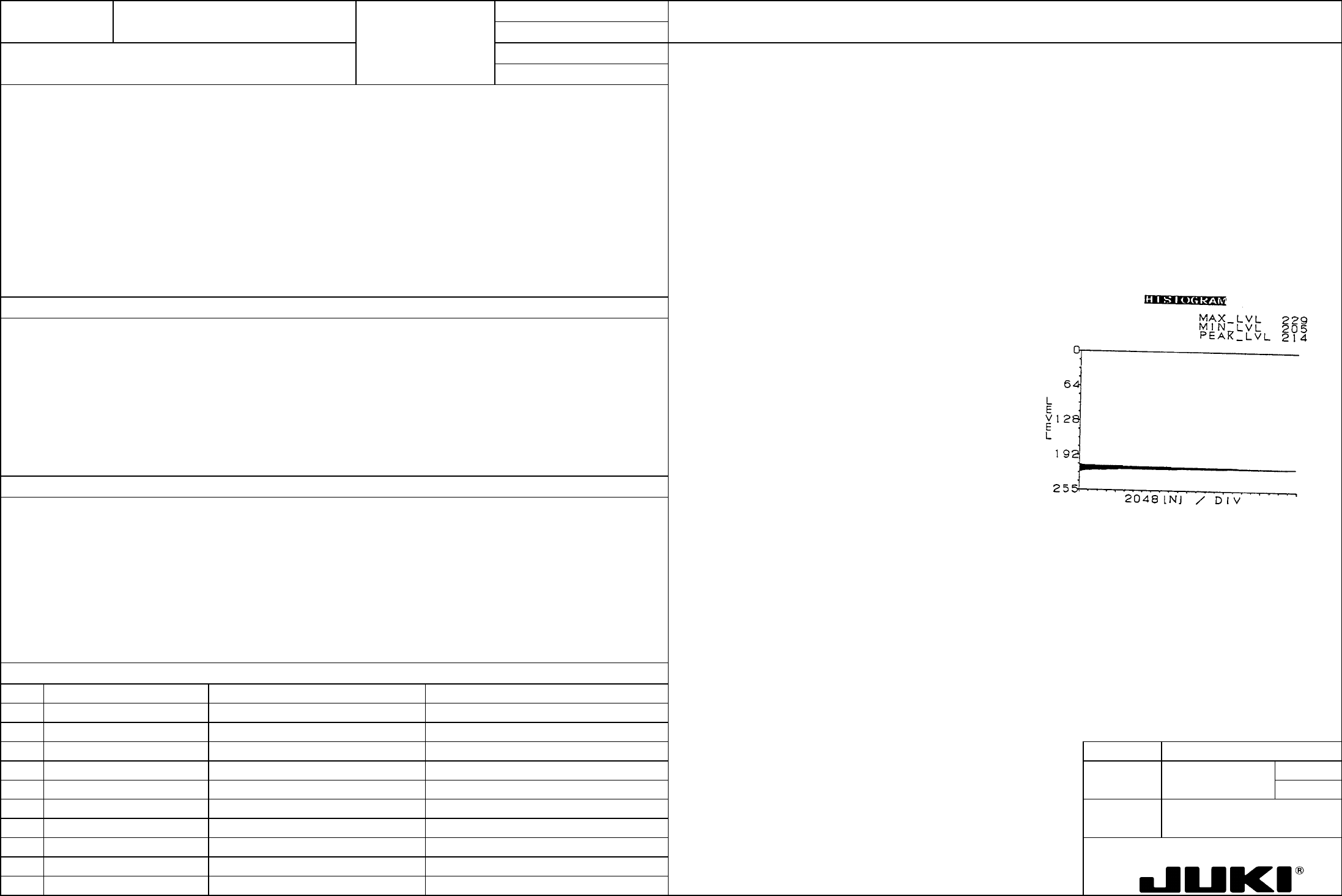
Histogram PEAK_LVL = 0.92 x MAX_LVL ±5
2. Turn ON OCC light R.
3. Turn VR6 of the base unit board so that OCC light R becomes the brightest.
4. Place a ceramic PWB (white) at a position about 10 mm from the leading edge of the LED of OCC light R. (At this time,
ensure that OCC light R runs parallel with the ceramic PWB.)
5. Show the histogram (as shown below on the right) under the condition of 4 and record the MAX_LVL value at that time.
6. With the ceramic PWB clamped and positioned on the transport rails, move the head so that the OCC camera R can view
the center of the ceramic PWB.
7. Read histogram and turn VR6 of the base unit board to obtain the specified PEAK_LVL value.
Serving as the adjustment of brightness of lighting for recognition of feeder bank mark, it affects the image taken in through the
recognition process.
1. Feeder bank mark recognition error
2. Error in the automatically calculated pickup position value for feeder bank position correction
FUNCTION NAME 0.4 VCS, 0.3 VCS Light Map Function/Performance CHECK/ADJUSTMENT METHODS (REMEDIAL ACTION PROCEDURE)
ASSURED QUALITY Reliability
QUALITY CHARACTERISTICS (SPECIFICATION VALUES) CATEGORY Safety
Product Image
ROLE IN FUNCTION (MEANING OF SPECIFICATION VALUES)
POSSIBLE MALFUNCTIONS (CAUSED BY INCORRECT SPECIFICATION VALUES)
COMPONENTS
NO. Part No. Part Name Associated Quality Characteristics
1 E86067250A0 Base unit board assembly DC power source output voltage adjustment
2 E86157210A0 0.4 VCS light board assembly
3 E86527210A0 0.3 VCS light board assembly MODEL KE-750/760
4 UNIT Electrical REF. NO.
5
NAME
EL-11
6 FUNCTION 0.4 VCS, 0.3 VCS Light Map 1/5
7
NAME
8
9
10
QA Table
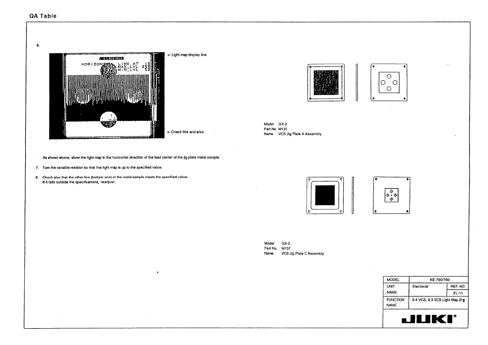
The same light adjustment procedure is used for 0.4 VCS and 0.3 VCS. Use the following adjustment jig and variable
resistors.
The light map must meet the following three requirements:
1. 30 ≤ MIN_LVL ≤ 40
(Either upper or lower part of the line of light map)
2. 230 ≤ MAX_LVL ≤ MAX_LVLsat
Application Adjustment jig Adjusting variable resistor
(Black acrylic only on background at measurement)
0.4 VCS VCS jig plate A assembly (part no. M131) Base unit board VR2
3. The difference between the max. and min. of the peak level is within 5 graduations
(as small as possible).
0.3 VCS VCS jig plate C assembly (part no. M137) Base unit board VR3
Within 5
graduations
Clean the metal sample of the VCS jig plate with alcohol to ensure that it is free of dirt and fingerprints.
1. Before starting the adjustment procedure, make sure that the DC power source output voltage has been properly adjusted.
2. Place the VCS light adjustment jig on the VCS light.
3. Turn ON the VCS light and turn the variable resistor to obtain the greatest intensity of the light.
Serving as the adjustment of lighting brightness for image recognition, it is directly concerned with the image taken in through
the recognition process, greatly affecting placement accuracy.
4. <- Light map display line
Take the light map in the horizontal direction of the body of the jig plate metal sample as
shown on the left.
5. <- Saturation
The above light map is displayed as shown on the left. Record the MAX_LVL at this time as
MAX_LVLsat.
1. Degraded placement accuracy when image recognition is used.
2. Image recognition error