IPC-7527.pdf - 第11页
5.1.2 Misregistration of Solder Paste Deposits Target – Class 1, 2, 3 • Paste deposit is centered on solder pad (Figures 5-6 and 5-7). • The paste deposit appears as one single block (unless segmented by design). • All s…
Control of the deposited amount ensures that the design
amount is obtained with reference to the thickness and
aperture of stencil. However, total weight of the assembly
cannot take the place of measurement of individual paste
deposits. Weight is only used for total volume assessment.
To weigh the boards, weigh clean, bare boards. Deposit the
paste using the normal print process. Then weigh the same
board again to determine the difference between the clean
board and the printed board. The difference will be the total
volume of paste applied to the board.
It is recommended to use a calibrated and accurate scale.
The accuracy of the scale will be determined according to
the size and density of the board assembly.
5 SHAPE OF SOLDER PASTE DEPOSIT
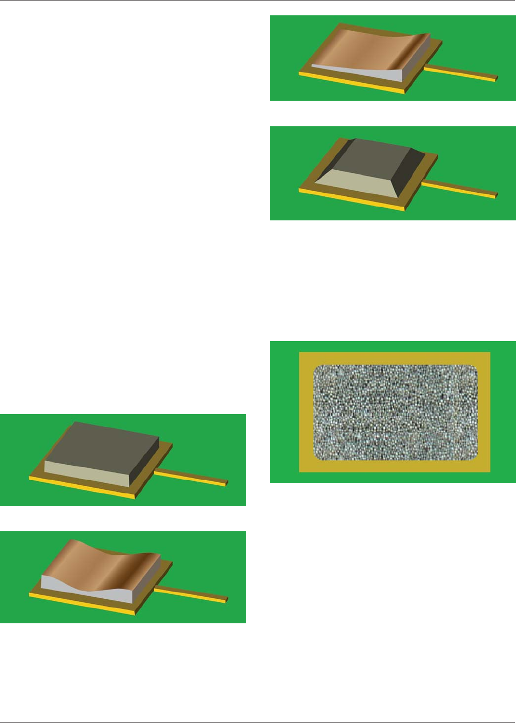
The volume and placement precision of the solder paste
deposits are the important factors for a correct solder paste
deposit. Ideally the paste deposit should have the same
shape as the stencil aperture (area and height). However, to
some extent it will be acceptable with varying paste deposit
shapes. See the appendix for possible shapes.
The paste deposit shape can be defined as follows:
• Full Shape (Figure 5-1)
• Saddle Shape (Figure 5-2)
• Roof Top Shape (Figure 5-3)
• Pyramid Shape (Figure 5-4)
5.1 Solder Paste Deposit – Misalignment A process
control system is recommended to ensure the lowest pos-
sible error rate, e.g., Statistical Process Control (SPC).
5.1.1 Slump
Target – Class 1, 2, 3
• Full shape solder paste deposit (Figure 5-5).
Acceptable – Class 1
• The paste deposit deviates from the nominal shape but
has the designed shape and volume.
Acceptable – Class 2, 3
• The paste deposit deviates from the designed shape but
slumps less than 25% in the X and Y directions.
Defect – Class 1
• Paste has connected with adjacent deposits.
Defect – Class 2, 3
• The paste has slumped more than 25% in the X and/or Y
directions.
Figure 5-1 Full Shape
Figure 5-2 Saddle Shape
Figure 5-3 Roof Top Shape
Figure 5-4 Pyramid Shape
Figure 5-5 Full Shape
IPC-7527 May 2012
4
SINGLE USER LICENSE - NOT FOR USE ON A NETWORK OR ONLINE
5.1.2 Misregistration of Solder Paste Deposits
Target – Class 1, 2, 3
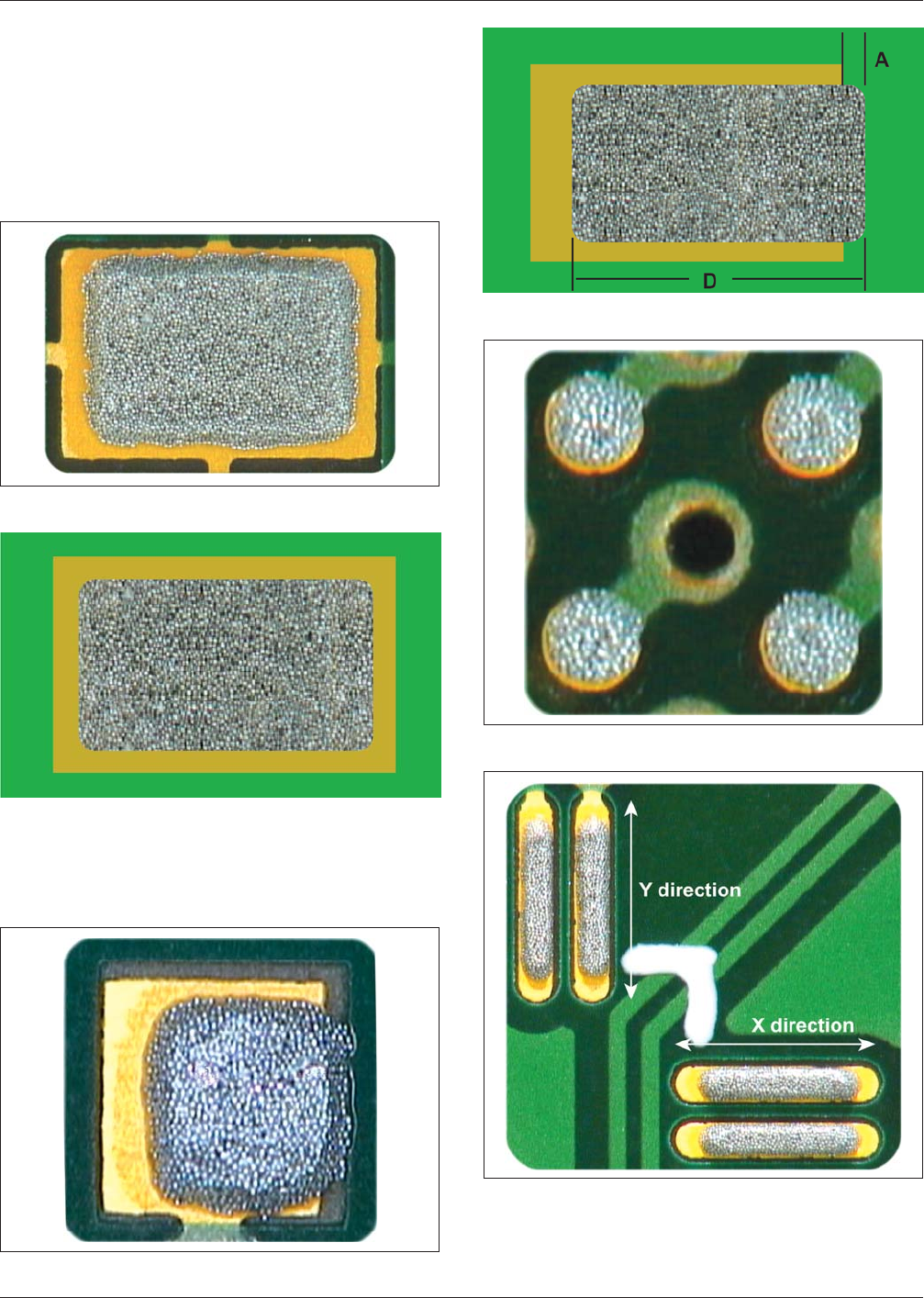
• Paste deposit is centered on solder pad (Figures 5-6 and
5-7).
• The paste deposit appears as one single block (unless
segmented by design).
• All solder balls have contact to the solder paste deposit.
Acceptable – Class 1, 2, 3
• Paste deposit (D) is off pad <25% (A) in X and/or Y
direction (Figures 5-8 through 5-13).
Figure 5-6 Centered Deposit
Figure 5-7 Centered Deposit
Figure 5-8 Offset – Acceptable
Figure 5-9 Offset – Acceptable
Figure 5-10 Offset – Acceptable
Figure 5-11 Offset – Acceptable
May 2012 IPC-7527
5
SINGLE USER LICENSE - NOT FOR USE ON A NETWORK OR ONLINE
Defect – Class 1, 2, 3
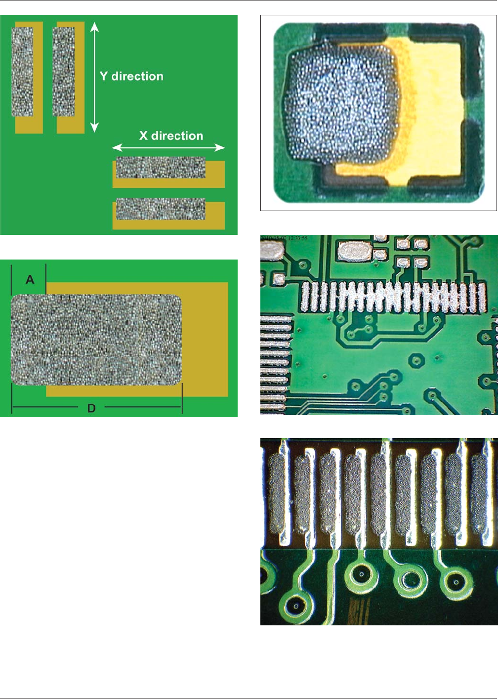
• Solder paste deposit has connected with adjacent pad
(Figure 5-15).
• Paste deposit (D) is off pad >25% (A) in X and/or Y
direction (Figures 5-14 through 5-16).
• Solder deposit not in single block (except by design).
• Solder balls that do not contact the solder paste deposit.
Figure 5-12 Offset – Acceptable
Figure 5-13 Offset – Acceptable
Figure 5-14 Offset – Defect
Figure 5-15 Shorting – Defect
Figure 5-16 Offset – Defect
IPC-7527 May 2012
6
SINGLE USER LICENSE - NOT FOR USE ON A NETWORK OR ONLINE