IPC-7527.pdf - 第15页
Appendix A Guideline for Operator Troubleshooting in the Solder Paste Screen Printing Process This section can be used as a guideline, so that the operator/user can identify error types and problem areas with relevant so…
5.1.4 Solder Paste Deposit – Height It may be neces-
sary to use a measurement system to evaluate this factor.
See Section 4, MEASUREMENT OF SOLDER PASTE
DEPOSITS.
Example of Tolerance:
• Component pin co-planarity: 100 µm [0.0039 in]
• Stencil thickness: 127 µm [0.005 in]
• Reduction of 20%
• Result of theoretical paste deposit height: 102 µm
[0.004 in]
See Appendix A for further examples.
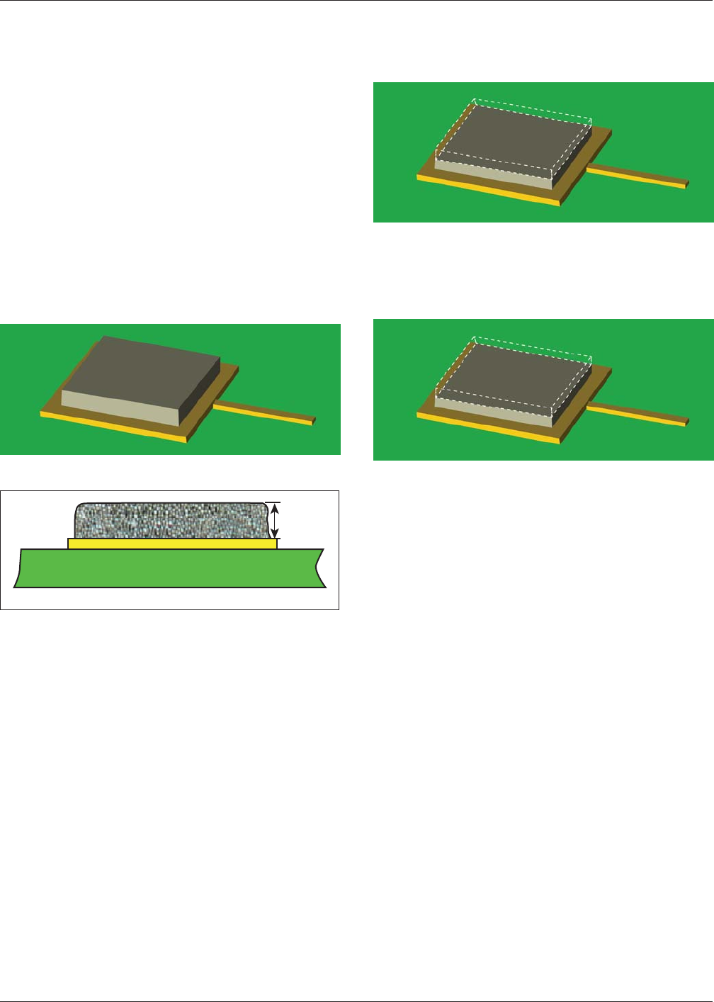
Target – Class 1, 2, 3
• Nominal height is achieved, (deposit height = stencil
thickness) (Figures 5-22 and 5-23).
Process Indicator – Class 1, 2, 3
• Paste deposit height 75% of stencil thickness (Figure
5-24).
Defect – Class 1, 2, 3
• Paste deposit height 50% of stencil thickness (Figure
5-25).
Figure 5-22 Height – Target
IPC-7527-5-23
Figure 5-23 Height – Target
Figure 5-24 Height – Process Indicator
Figure 5-25 Height – Defect
IPC-7527 May 2012
8
SINGLE USER LICENSE - NOT FOR USE ON A NETWORK OR ONLINE
Appendix A
Guideline for Operator Troubleshooting in the
Solder Paste Screen Printing Process
This section can be used as a guideline, so that the
operator/user can identify error types and problem areas
with relevant solutions that can be used in connection with
correcting/optimizing of the solder paste deposits.
The following requirements should be met before the
screen printer process optimization can be started:
• The solder paste should meet the requirements of J-STD-
005 or equivalent.
• The stencil should be in good condition and have the cor-
rect tension.
• The squeegee blades/printing head should be in good con-
dition and mounted correctly.
• There should be sufficient board support for the PCB dur-
ing the printing process.
• The stencil should be clean on both sides and in the aper-
tures (inspect with microscope).
A.1 Visual Check for Solder Paste Printing Optimization
• Does the solder paste roll when pushed by the squeegee
blades?
• Are all apertures filled 100% with solder paste?
• Is the top side of the stencil free of solder paste residues?
• Is the solder paste released from the stencil apertures?
• Is there solder paste residues on the bottom side of the
stencil?
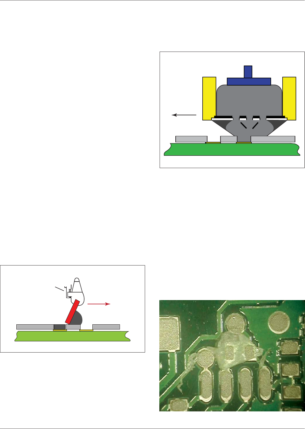
A.2 Tolerances The nominal solder paste deposit height
equals the stencil thickness. However, this will not always
be true because of other factors that influence the paste
deposit height such as solder mask, silk screen, labels,
masking, and contaminates on the PCB surface (Figures
A-3 and A-4).
Note: There may be differences in the solder deposit
depending on the type of squeegee blade used; e.g., metal,
rubber or plastic. The customer and manufacturer should
agree on the acceptable conditions when other than metal
blades are used.
IPC-7527-A-1
Figure A-1 Solder Paste Printing with Squeegee Blades
1. Squeegee Pressure
2. Blade Height
3. Squeegee Speed
4. Paste
5. Squeegee
kg
1
2
3
4
PCB
Stencil
5
IPC-7527-A-2
Figure A-2 Solder Paste Printing with Enclosed Head
System
1. Printing Speed
2. Enclosed Head
3. Paste Pressure
1
3
2
Figure A-3 Plastic from Packaging
May 2012 IPC-7527
9
SINGLE USER LICENSE - NOT FOR USE ON A NETWORK OR ONLINE
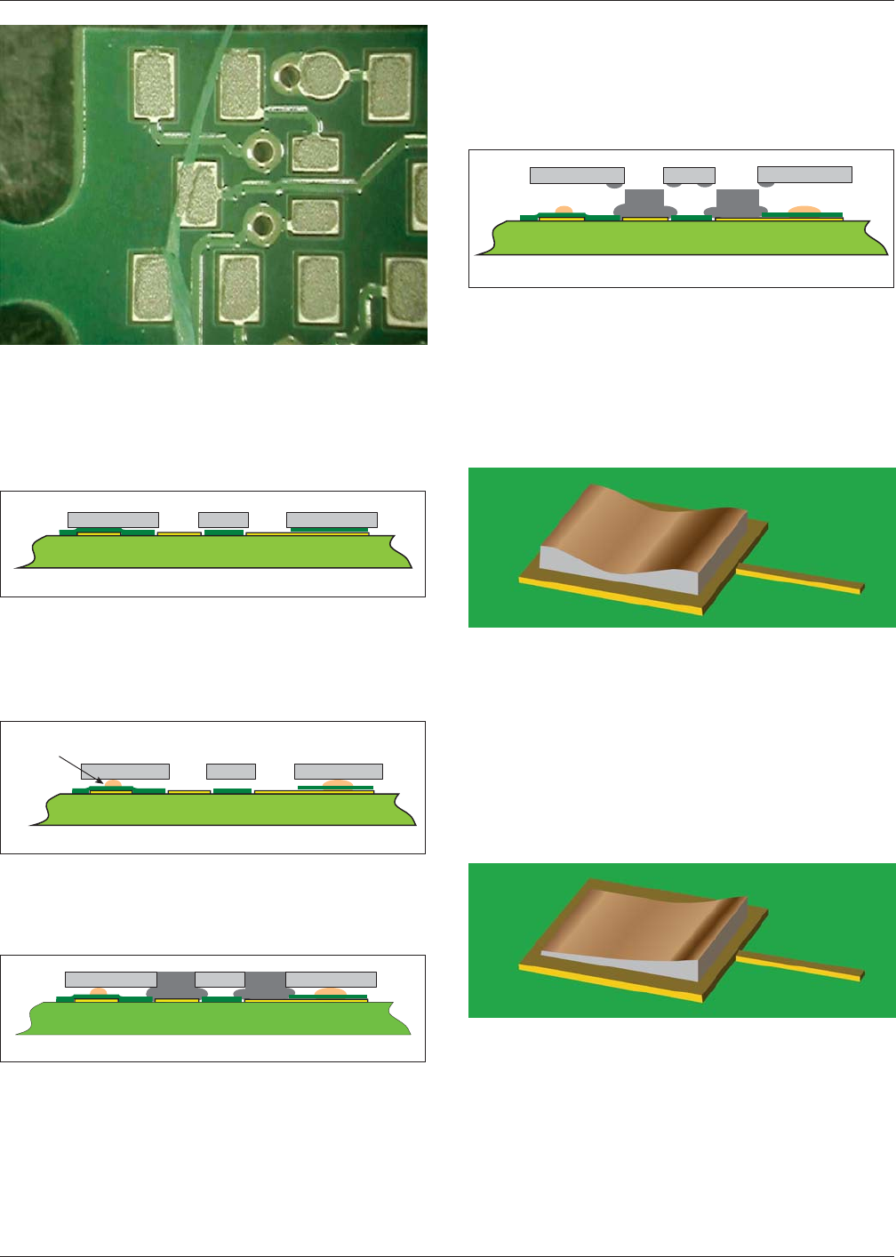
Figure A-5 illustrates the effect of solder mask. Due to sol-
der mask coverage on the tracks, the stencil will be lifted.
Result: Increased height of solder paste deposit and solder
paste smearing.
Figure A-6 illustrates the effect when solder mask is com-
bined with silk screen. This gives a further increase in the
paste deposit height and smearing.
Figure A-7 illustrates the effect of solder paste smearing
resulting in solder balls after the reflow process.
When the solder paste smears, a small amount of paste will
be left on the bottom side of the stencil (Figure A-8), which
may then be deposited on the next PCB. This problem can
be reduced by cleaning the bottom side of the stencil.
There are automatic cleaning systems that can be fixed into
the screen printer; these can be programmed so that the
stencil is cleaned with fixed intervals or as required. See
Section A.8, Issues with Stencil Cleaning.
A.3 Varying Paste Deposit Shape This section is a
guideline to suggest possible causes of the listed problems.
It is not intended to be a corrective action checklist.
Problem A.3.1 Saddle Shape Paste Deposit
(Figure A-9)
Possible causes:
• Printing pressure too high.
• Squeegee blades too soft.
• Aperture area too large compared to squeegee type and
pressure.
Problem A.3.2 Roof Top Shape Paste Deposit
(Figure A-10)
Possible causes:
• Solder paste is not rolling during printing.
• Print speed too high.
• Insufficient solder paste on stencil.
Figure A-4 Glass Fiber from PCB
IPC-7527-A-5
Figure A-5 Effect of Solder Mask
PCB
Stencil
IPC-7527-A-6
Figure A-6 Effect of Silk Screen
PCB
Stencil
Silk Screen
IPC-7527-A-7
Figure A-7 Effect of Solder Paste
PCB
Stencil
IPC-7527-A-8
Figure A-8 Result of Silk Screen Interference
PCB
Stencil
Figure A-9 Saddle Shape Deposit
Figure A-10 Roof Top Shape Paste Deposit
IPC-7527 May 2012
10
SINGLE USER LICENSE - NOT FOR USE ON A NETWORK OR ONLINE