IPC-7527.pdf - 第7页
Requirements for Solder Paste Printing 1 GENERAL 1.1 Scope This standard is a collection of visual quality acceptability criteria for solder paste printing. 1.2 Purpose The purpose of this guideline document is to suppor…

Table of Contents
1 GENERAL ................................................................... 1
1.1 Scope .................................................................... 1
1.2 Purpose ................................................................. 1
1.3 Background .......................................................... 1
1.4 Terms and Definitions ......................................... 1
1.4.1 Classification ........................................................ 1
1.4.2 Disposition* ......................................................... 1
1.4.3 Slumping .............................................................. 1
1.4.4 Combined Conditions .......................................... 1
1.4.5 Designed Volume ................................................. 1
1.5 Specialized Designs ............................................. 1
1.6 Verification of Dimensions .................................. 2
1.7 Magnification Aids ............................................... 2
1.8 Lighting ................................................................ 2
2 APPLICABLE DOCUMENTS .................................... 2
2.1 IPC ....................................................................... 2
2.2 ASTM ................................................................... 2
3 CHOICE OF TECHNOLOGY .................................... 2
4 MEASUREMENT OF SOLDER PASTE
DEPOSITS
................................................................. 3
5 SHAPE OF SOLDER PASTE DEPOSIT .................. 4
5.1 Solder Paste Deposit – Misalignment ................. 4
5.1.1 Slump ................................................................... 4
5.1.2 Misregistration of Solder Paste Deposits ............ 5
5.1.3 Solder Paste Deposit – Area ............................... 7
5.1.4 Solder Paste Deposit – Height ............................ 8
Appendix A Guideline for Operator Trouble-
shooting in the Solder Paste
Screen Printing Process
....................... 9
Figures
Figure 3-1 Squeegee Blade ............................................... 2
Figure 3-2 Enclosed Paste Print Head .............................. 3
Figure 3-3 Needle Dispense .............................................. 3
Figure 3-4 Paste Jet Dispense .......................................... 3
Figure 4-1 Sample of an Automated Machine Readout .... 3
Figure 4-2 Sample of an Automated Inspection Result ..... 3
Figure 4-3 Weighing Solder Paste ..................................... 3
Figure 5-1
Full Shape ........................................................ 4
Figure 5-2
Saddle Shape ................................................... 4
Figure 5-3
Roof Top Shape ................................................ 4
Figure 5-4
Pyramid Shape ................................................. 4
Figure 5-5
Full Shape ........................................................ 4
Figure 5-6 Centered Deposit .............................................. 5
Figure 5-7 Centered Deposit .............................................. 5
Figure 5-8 Offset – Acceptable .......................................... 5
Figure 5-9 Offset – Acceptable .......................................... 5
Figure 5-10 Offset – Acceptable .......................................... 5
Figure 5-11 Offset – Acceptable .......................................... 5
Figure 5-12 Offset – Acceptable .......................................... 6
Figure 5-13 Offset – Acceptable .......................................... 6
Figure 5-14 Offset – Defect .................................................. 6
Figure 5-15 Shorting – Defect .............................................. 6
Figure 5-16 Offset – Defect .................................................. 6
Figure 5-17 Area – Target .................................................... 7
Figure 5-18 Area – Target .................................................... 7
Figure 5-19 Area – Acceptable ............................................ 7
Figure 5-20 Area – Acceptable ............................................ 7
Figure 5-21 Area – Defect ................................................... 7
Figure 5-22 Height – Target ................................................. 8
Figure 5-23 Height – Target ................................................. 8
Figure 5-24 Height – Process Indicator ............................... 8
Figure 5-25 Height – Defect ................................................. 8
Figure A-1 Solder Paste Printing with Squeegee
Blades ............................................................... 9
Figure A-2 Solder Paste Printing with Enclosed Head
System .............................................................. 9
Figure A-3 Plastic from Packaging ..................................... 9
Figure A-4 Glass Fiber from PCB .................................... 10
Figure A-5 Effect of Solder Mask ..................................... 10
Figure A-6 Effect of Silk Screen ....................................... 10
Figure A-7 Effect of Solder Paste ..................................... 10
Figure A-8 Result of Silk Screen Interference ................. 10
Figure A-9 Saddle Shape Deposit .................................... 10
Figure A-10 Roof Top Shape Paste Deposit ...................... 10
Figure A-11 Spikes on Paste Deposit ................................ 11
Figure A-12 Increased Deposit Quantity ............................ 11
Figure A-13 Decreased Quantity ........................................ 11
Figure A-14 Slumping/Smearing ......................................... 11
Figure A-15 Paste Residues .............................................. 12
Figure A-16 Long Smear .................................................... 12
Figure A-17 Offset .............................................................. 12
Figure A-18 Excess Residue Along Direction of Travel ..... 12
Figure A-19 Residue Across Direction of Travel ................ 13
Figure A-20 Solder Balls .................................................... 13
Figure A-21 Close Up of Solder Balls ................................ 13
Tables
Table 1-1 Inspection Magnification (Land Width) ................ 2
IPC-7527 May 2012
iv
SINGLE USER LICENSE - NOT FOR USE ON A NETWORK OR ONLINE

Requirements for Solder Paste Printing
1 GENERAL
1.1 Scope
This standard is a collection of visual quality
acceptability criteria for solder paste printing.
1.2 Purpose The purpose of this guideline document is
to support the user in the visual evaluation of the solder
paste printing process, which makes subsequent process
optimizing possible.
The purpose of this guideline is not to inspect and evaluate
the quality of the solder paste. For information on the
evaluation of solder paste, see J-STD-005, Requirements
for Soldering Pastes and IPC-HDBK-005.
The purpose is not to define requirements to stencil design.
For information on stencil design, see IPC-7525, Stencil
Design Guideline.
Appendix A provides different error types and suggested
solutions are listed. The guideline is intended to help/
improve the optimizing process for paste printing.
In the case of a discrepancy, the description or written
criteria always takes precedence over the illustrations.
1.3 Background Standards such as J-STD-001 and IPC-
A-610 provide tools that help to promote quality within the
electronics industry. However, the standards do not include
requirements of visual appearance of the paste deposit. The
industry has, for some time, expressed a wish for a stan-
dard to support the users in the solder paste printing pro-
cess. IPC-7527 will help improve the quality in this very
sensitive process.
1.4 Terms and Definitions Other than those terms listed
below, the definitions of terms used in this standard are in
accordance with IPC-T-50. Terms quoted from IPC-T-50
are marked with *.
1.4.1 Classification
CLASS 1 General Electronic Products
Includes products suitable for applications where the major
requirement is function of the completed assembly.
CLASS 2 Dedicated Service Electronic Products
Includes products where continued performance and
extended life is required, and for which uninterrupted ser-
vice is desired, but not critical. Typically the end-use envi-
ronment would not cause failures.
CLASS 3 High Performance Electronic Products
Includes products where continued high performance or
performance-on-demand is critical, equipment downtime
cannot be tolerated, or the end-use environment may be
uncommonly harsh.
Target Condition A condition that is close to perfect/
preferred, however, it is a desirable condition and not
always achievable and may not be necessary to ensure reli-
ability of the assembly in its service environment.
Acceptable Condition Indicates a condition that, while not
necessarily perfect, will maintain the integrity and reliabil-
ity of the assembly in its service environment.
Defect Condition A condition that may be insufficient to
ensure the form, fit, or function of the assembly in its end
use environment. Defect conditions shall be dispositioned
by the manufacturer based on design, service, and customer
requirements. Disposition may be to rework, repair, scrap,
or use as is. Repair or use as is may require customer con-
currence.
A defect for Class 1 automatically implies a defect for
Class 2 and 3. A defect for Class 2 implies a defect for
Class 3.
1.4.2 Disposition* The determination of how defects
should be treated. Dispositions include, but are not limited
to, rework, use as is, scrap, or repair.
1.4.3 Slumping Solder paste flows out after it is applied.
See more in IPC-HDBK-005.
1.4.4 Combined Conditions There may be situations
where a combination of maximum deviations in form,
placement, coverage, and height can result in lack of sol-
dering or wrong amount of solder paste. The manufacturer
is responsible for identification of such conditions.
1.4.5 Designed Volume The designed volume is equal to
the area of the stencil aperture times the stencil thickness
(volume = length x width x height). Volume is not a visu-
ally inspectable condition.
1.5 Specialized Designs This standard, as an industry
consensus document, cannot address all of the possible
components and product design combinations. Where
uncommon or specialized technologies are used, it may be
necessary to develop unique acceptance criteria. However,
where similar characteristics exist, this document may pro-
vide guidance for product acceptance criteria. Often,
unique definition is necessary to consider the specialized
characteristics while considering product performance cri-
teria. The development should include customer involve-
ment or consent. For Class 3, the criteria shall include
agreed definition of product acceptance.
May 2012 IPC-7527
1
SINGLE USER LICENSE - NOT FOR USE ON A NETWORK OR ONLINE
Whenever possible these criteria should be submitted to the
IPC Technical Committee to be considered for inclusion in
upcoming revisions of this standard.
1.6 Verification of Dimensions The actual measure-
ments provided in this document (i.e., specific part mount-
ing and solder fillet dimensions and determination of per-
centages) are not required except for referee purposes. All
dimensions in this standard are expressed in SI (System
International) units (with Imperial English equivalent
dimensions provided in brackets). All specified limits in
this standard are absolute limits as defined in ASTM E29.
1.7 Magnification Aids For visual inspection, some indi-
vidual specifications may call for magnification aids for
examining solder paste print.
The tolerance for magnification aids is ± 15% of the
selected magnification power. Magnification aids, if used
for inspection, shall be appropriate for the item being
inspected. Unless magnification requirements are otherwise
specified by contractual documentation, the magnifications
in Table 1-1 are determined by the item being inspected.
Referee conditions are used to verify product rejected at
the inspection magnification power. For assemblies with
mixed land widths, the greater magnification may be used
for the entire assembly.
1.8 Lighting Lighting shall be adequate for the item
being inspected.
Illumination at the surface of workstations should be at
least 1000 lm/m
2
[approximately 93 foot candles]. Light
sources should be selected to prevent shadows.
Note: In selecting a light source, the color temperature of
the light is an important consideration. Light ranges from
3000-5000° K enable users to distinguish various solder
paste printing features and contaminates with increased
clarity.
2 APPLICABLE DOCUMENTS
The following documents currently in effect form a part of
this specification to the extent specified herein.
2.1 IPC
1
IPC-J-STD-005 Requirements for Soldering Pastes
IPC-HDBK-005 Guide to Solder Paste Assessment
IPC-T-50 Terms and Definitions for Interconnecting and
Packaging Electronic Circuits
IPC-A-610 Acceptability of Electronic Assemblies
IPC-7525 Stencil Design Guidelines
IPC-7526 Stencil and Misprinted Board Cleaning Hand-
book
2.2 ASTM
2
ASTM E29 Standard Practice for Using Significant Digits
in Test Data to Determine Conformance with Specifica-
tions.
3 CHOICE OF TECHNOLOGY
The requirements in this standard have been developed for
solder paste printing. Since the requirements are referred to
as general, it is also possible to evaluate other application
methods according to this standard. However, it may be
necessary to develop specific acceptance requirements for
the chosen application method.
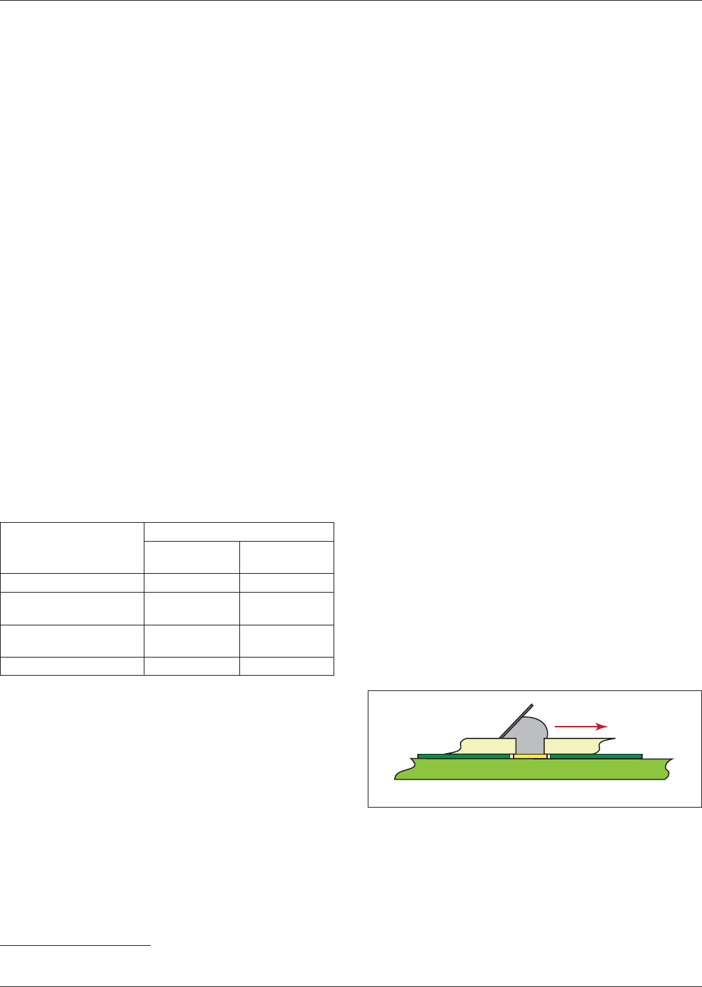
Various methods can be used when solder paste is applied
to the PCB (printed circuit board). Four methods are illus-
trated here:
• Squeegee Blade (Figure 3-1)
• Enclosed Print Head (Figure 3-2)
• Needle Dispense (Figure 3-3)
• Paste Jet Dispense (Figure 3-4)
1. www.ipc.org
2. www.astm.org
Table 1-1 Inspection Magnification (Land Width)
Land Widths or
Land Diameters
Magnification Power
Inspection
Range
Maximum
Referee
>1.0 mm [0.0394 in] 1.5X to 3X 4X
>0.5 to ≤1.0 mm
[0.0197 to 0.0394 in]
3X to 7.5X 10X
≥0.25 to ≤0.5 mm
[0.00984 to 0.0197 in]
7.5X to 10X 20X
<0.25 mm [0.00984 in] 20X 40X
IPC-7527-3-1
Figure 3-1 Squeegee Blade
1. Squeegee
2. Paste
3. Stencil
4. PCB
1
23
4
IPC-7527 May 2012
2
SINGLE USER LICENSE - NOT FOR USE ON A NETWORK OR ONLINE