Specification_SIPLACE_S23HM_eng.pdf - 第20页
19 Description In cluster technology, each sub- panel is as signed an in k spot. If this is present when the PCB vi- sion module conducts the meas- urement, the pertinent subpanel is not populated. Naturally, it is also …
18
Description
Different reference mark shapes
prove to be optimal depending on
the condition of the surface.
Particularly advisable for bare cop-
per surfaces with little oxidation is
the single cross. Maximum recog-
nition reliability is achieved due to
the high information content. Rec-
tangle, square and circle are less
”informative” but save space, are
rugged, and can even be used
when oxidation is at an advanced
stage.
Advisable for tinned structures are
circle or square because in this
case the ratio of the mark dimen-
sions to the presolder thickness is
particularly favorable.
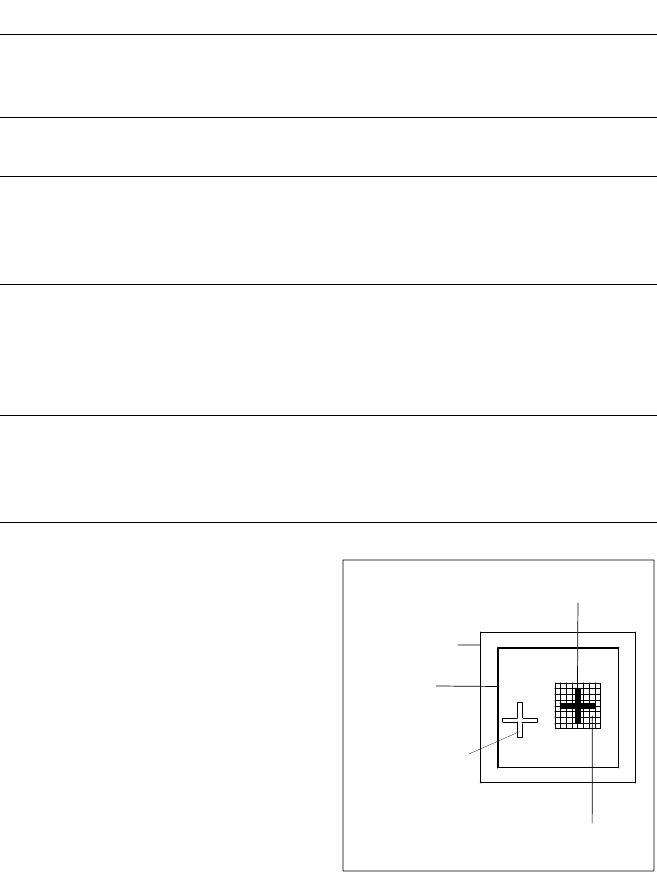
Vision Sensor Technology:
PCB Position Recognition
Template
Window
PCB Camera
Field of View
Search
Area
Fiducial to
Be Located
Reference
Fiducal
Reference Mark Criteria
Locate 2 marks
Locate 3 marks in addition
X-/Y-position, rotation angle, mean dis-
tortion
Shear, distortion in X- and Y-direction
Mark shapes Freely definable via teaching, e.g.,
single cross, rectangle, square, circle
Mark surface
Copper
Tin
Without oxidation and solder resist
Warp ≤ 1/10 of structure width,
good contrast to environment
Mark dimensions
single cross
rectangle/square
circle
Length and width: 0.9 - 2 mm
Line thickness: 0.3 - 1.0 mm
Edge length: 0.5 - 2 mm
Diameter: 0.5 - 2 mm
Mark environment Clearance around reference mark not
necessary if there is no similar mark
structure in the search area
(5.7 x 5.7 mm)

19
Description
In cluster technology, each sub-
panel is assigned an ink spot. If
this is present when the PCB vi-
sion module conducts the meas-
urement, the pertinent subpanel is
not populated.
Naturally, it is also possible to pre-
vent the population of the sub-
panel when the ink spot is miss-
ing.
This function can be used to pre-
vent costs incurred by unneces-
sarily populating faulty subpanels.
P
PP
Po
oo
os
ss
si
ii
it
tt
ti
ii
io
oo
on
n n
n R
RR
Re
ee
ec
cc
co
oo
og
gg
gn
nn
ni
ii
it
tt
ti
ii
io
oo
on
n n
n o
oo
of
f f
f F
FF
Fee
eeee
eed
dd
de
ee
er
rr
r
The pick-up position of the com-
ponents can be determined pre-
cisely with the aid of the position
recognition of the feeder. It is acti-
vated each time after a change of
feeder or component table. The
offset in position relative to the
stored ideal position is determined
on the basis of fiducials on the
feeder modules using the PCB vi-
sion module. This provides a very
high pick-up reliability even for the
very first component. This is par-
ticularly important with small com-
ponents.
Vision Sensor Technology:
Recognition of Faulty PCBs via Ink Spots
Position Recognition of Feeder
Ink Spot Criteria
Mark shapes Single cross (recommended because
of lowest susceptibility to problems),
rectangle, square, circle, etc.
Masking material Mat dark (light-absorbent)
Not advisable: white or glossy
Size of mark masking
Circular: Diameter ≥ 8.1 mm
Square: Edge length ≥ 5.7 mm
Mark recognition time
(Travel > 100 mm)
Mark masked: 1.2 s
Mark not masked: 0.4 s

20
Description
The component vision module is
directly integrated into the revolver
head and it takes a picture of the
pertinent component. This image
is analyzed by the central vision
system while the component is
cycling into the next station, where
the position of the component is
corrected in accordance with the
offsets in position discovered.
Vision Sensor Technology:
Component Vision Module on the 12-Nozzle Revolver Head
Technical Data
Maximum component size 18.7 x 18.7 mm
Recognizable spectrum
of components
0402 to PLCC44
incl. BGA, µBGA, Flip Chip, TSOP,
QFP, PLCC, SO to SO32, DRAM
Lead pitch
min. ≥ 0.5 mm
Camera’s field of view 24 x 24 mm
Type of lighting Front lighting
(3 freely programmable planes)