西门子SIPLACE HS 60-设备参数_EN.pdf - 第14页
12 PCB Conveyor: Ceramic Substrate Centering (Option) Stopper Technical Data Stopper Ceramic Substrate Movable Conveyor Side Movable Conveyor Side Stationary Conveyor Side Stationary Conveyor Side Ceramic Substrate X- Ce…
11
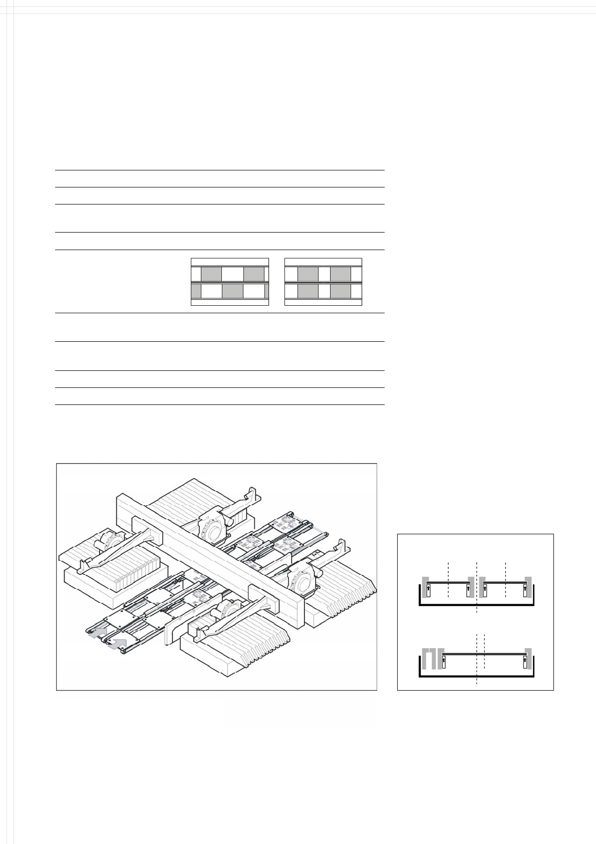
PCB Conveyor:
Flexible Dual Conveyor
Technical Data
Description
Thanks to reduced non-productive
times the dual PCB conveyor can
substantially increase the through-
put, depending on the program. It
makes it possible to transport two
PCBs through the machine.
PCB dimensions See table on page 3
Fixed conveyor edge Right (standard), left (option)
Asynchronous and Synchronous Transport on Dual Conveyor
Transport mode Asynchronous Synchronous
View
Placement program
per conveyor
same or different same or different
PCB width
per conveyor
same same or different
Ink spot recognition possible not possible
Automatic width adjustment possible not possible
Asynchronous transport
A PCB is moved into the machine
in “slack time” while the other
PCB is being populated. The non-
productive time caused by the PCB
transport is completely eliminated.
The increase in placement speed
reaches 30%, depending on the
components placed on the PCB.
Synchronous transport
Two PCBs are populated simul-
tanously. The real placement rate
can be increased, especially when
boards with only a few compo-
nents are handled.
PCB
Transport Direction
By use of Station Computer Soft-
ware 505.02 (or higher) the dual con-
veyor can be processed in single
conveyor mode, which allows the
handling of PCBs with a maximum
width up to 380mm (see table on
page 3).
Modus 1: Dual Conve
y
or
Modus 2: Single Conveyor
Dual Conveyor with Asynchronous Transport
Flexible Dual Conveyor
12
PCB Conveyor:
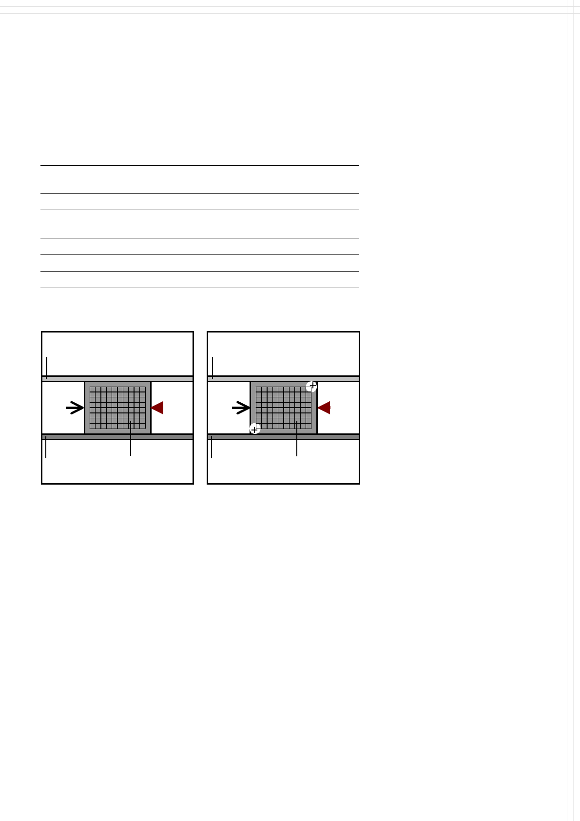
Ceramic Substrate Centering (Option)
Stopper
Technical Data
Stopper
Ceramic
Substrate
Movable
Conveyor Side
Movable
Conveyor Side
Stationary
Conveyor Side
Stationary
Conveyor Side
Ceramic
Substrate
X-
Centering
X-
Centering
Description
Some ceramic substrates can
be damaged by standard PCB
clamping. In this case the Ceramic
Substrate Centering can be used,
which fixes the substrate mecha-
nically. In general there is no need
for additional optical centering,
but nevertheless the accuracy will
be increased by using the PCB
camera to detect reference marks
(fiducials) on the substrate. For
ceramic substrate the SIPLACE
Multicolor Fiducial Camera (see
page 23) is recommended.
50 x 50 mm
2
to 101.6 x 177.8 mm
2
/
2" x 2" to 4" x 7"
Substrate dimensions
Substrate thickness 0.5 to 4.5 mm
Substrate model Unscribed (no difficulty)
Scribed (after test)
Contact in conveyor 2.5 mm
Substrate bottom clearance 12 mm
Compressed air connection 5.5 bar
X-Centering
Mechanical Centering Optical Centering via PCB Camera
13
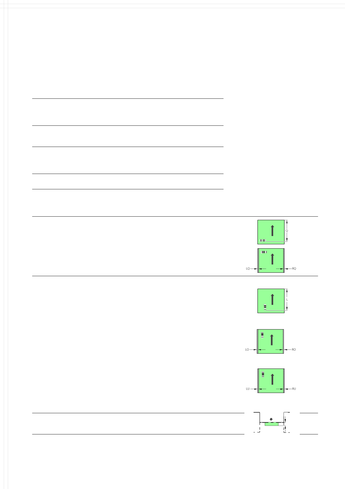
PCB Conveyor:
PCB Bar Code for Production-Controlled Manufacturing
(Option)
Technical Data
Label dimensions Stroke width: W: 0.19 < W ≤ 0.3 mm
(corresponds to high + medium density)
Stroke length: ≥ 4 mm a
Length of scanning window: ≤ 90 mm
Recommended
label colors
Color coding: black, dark green or dark blue
Background: white, beige, yellow, orange
(contrast ratio > 70% as per DIN 66236)
Code types Code 39, Code 128 / EAN 128, Codabar, 2/5 interleaved,
2/5 IATA 2/5 industrial, UPC, EAN, Pharma Code,
EAN Addendum (more upon request); max. 25 char-
acters, definition of a bar code filter possible
Safety of the
laser scanner
Laser diode 670 nm (red) / 1 mW
Laser protection class 2, degree of protection IP65
Restrictions Depending to sort of scanner (1D / 2D) as well as
orientation (along / across to transport direction) and
position of the bar code (top/bottom of PCB) distinct
distances have to be obeyed:
Bar code (BC)
ACROSS to
transport direction
Q = Distance
PCB front edge to
BC back border
RQ/LQ = Distance
PCB side edge to BC-side
border right/left
2D-scanner PCB top:
Q: max. 310 mm, RQ: min. 3 mm, LQ: min. 3 mm
2D-scanner PCB bottom:
Q: max. 310 mm, RQ: min. 5 mm, LQ: min. 5 mm
1D-scanner PCB top:
Q: max. 310 mm, RQ: min. 3 mm, LQ: min. 3 mm
1D-scanner PCB bottom:
Q: max. 310 mm, RQ: min. 5 mm, LQ: min. 5 mm
Barcode (BC)
ALONG
transport direction
L = Distance
PCB front edge to
BC back border
RO/LO = Distance
PCB side edge to BC-
side border right/left
(PCB top)
RU/LU = Distance
PCB side edge to BC-
side border right/left
(PCB bottom)
1D-scanner PCB top L: 240 - 310 mm,
• with single conveyor
standard 18" RO: min. 35 mm, LO: min. 3 mm
Option 20" RO: min. 61 mm, LO: min. 3 mm
• with dual conveyor, lane 1
standard 8,5" RO: min. 40 mm, LO: min. 3 mm
2x9,5"/1x430 RO: min. 66 mm, LO: min. 3 mm
• with dual conveyor, lane 2
standard 8,5" RO: min. 3 mm, LO: min. 3 mm
2x9,5"/1x430 RO: min. 3 mm, LO: min. 3 mm
1D-scanner PCB bottom L: 280 - 350 mm,
• with single conveyor
standard 18"/460 RU: min. 5 mm, LU: min. 35 mm
Option 20"/508 RU: min. 5 mm, LU: min. 61 mm
• with dual conveyor, lane 1
standard 8,5" RU: min. 5 mm, LU: min. 15 mm
2x9,5"/1x430 RU: min. 5 mm, LU: min. 15 mm
• with dual conveyor, lane 2
standard 8,5"/216 RU: min. 5 mm, LU: min. 40 mm
2x9,5"/1x430/250 RU: min. 5 mm, LU: min. 66 mm
Space required
for bar code in
transport direction
2D-scanner PCB bottom, lane 2
mechanical abundance over machine:
no abundance
Description
The SIPLACE PCB bar code scan-
ner supports the flexible produc-
tion of SMD products and en-
hances placement reliability. The
laser scanner reads the bar code
label on the top and/or bottom of
each PCB moving during transport.
On the basis of the bar code in-
formation the line computer auto-
matically selects the correct place-
ment program from the previously
prepared bar code assignment list
and sends it to the station.
The bar code filter can be utilized,
if only certain information con-
tained in the bar code is relevant.