西门子SIPLACE HS 60-设备参数_EN.pdf - 第24页
22 Vision Sensor Technology: Bad Board Recognition Position Recognition of Feeder Ink Spot Criteria Evaluation method for fiducials for structures brightness method contrast method Shapes and sizes of fiducials/structure…
21
Vision Sensor Technology:
PCB Position Recognition
Reference Mark Criteria
Locate 2 marks
Locate 3 marks in addition
X-/Y-position, rotation angle, mean distortion
Shear, distortion in X- and Y-direction
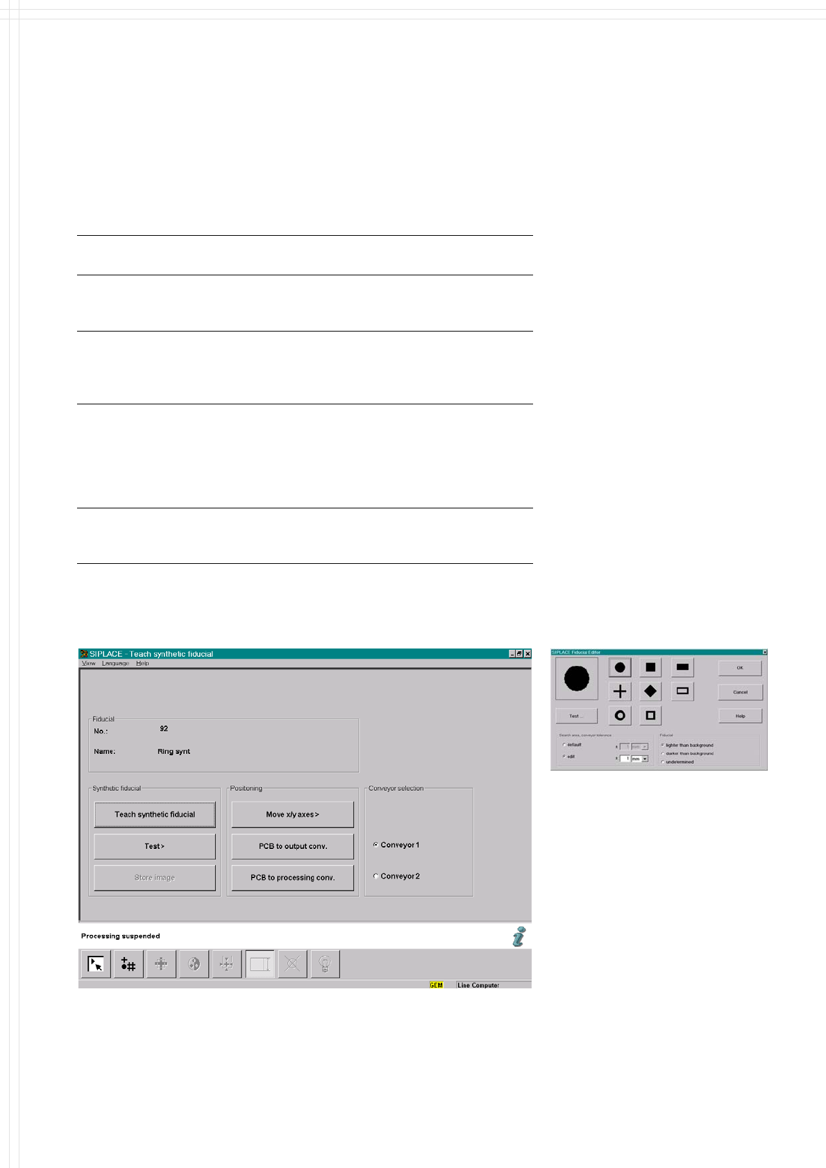
Mark shapes Synthetic marks e.g., circle, cross, square,
rectangle, rhombus, circular ring, square
ring, octagonal ring (choose from menu)
Mark surface:
Copper
Tin
Without oxidation and solder resist
Warp ≤ 1/10 of structure width,
both with good contrast to environment
Mark dimensions
Circle
Cross
Rectangle/square
Rhombus
Diameter: 0.3 - 3 mm
Length and width: 0.3 - 3 mm
Line thickness: 0.1 - 1.5 mm
Edge length: 0.3 - 3 mm
Transversal length: 0.3 - 3 mm
Mark environment Clearance around reference mark not
necessary if there is no similar mark
structure in the search area
Description
Different reference mark shapes
prove to be optimal depending on
the condition of the surface.
Particularly advisable for bare cop-
per surfaces with little oxidation is
the single cross. Maximum recog-
nition reliability is achieved due to
the high information content. Rec-
tangle, square and circle are less
“informative” but save space, are
rugged, and can even be used
when oxidation is at an advanced
stage.
Advisable for tinned structures are
circle or square because in this
case the ratio of the mark dimen-
sions to the presolder thickness is
particularly favorable.
Fiducial Editor
Teach Synthetic Fiducial

22
Vision Sensor Technology:
Bad Board Recognition
Position Recognition of Feeder
Ink Spot Criteria
Evaluation method
for fiducials
for structures
brightness method
contrast method
Shapes and sizes of
fiducials/structures for
brightness method
contrast method
square or circular forms
edge length/diameter 0.3 - 5 mm
rectangular forms
edge length 0.3 - 5 mm
Masking material mat dark (light-absorbing)
not recommended: white or shiny
Ink spot recognition time 0.3 s for each method
Description
In the cluster technology each
subpanel is assigned an ink spot.
If this is present during the meas-
urement via the PCB vision mod-
ule, the corresponding subpanel is
populated. It is also possible to ac-
complish the population of the
subpanel when the ink spot is
missing. With this function it is
possible to eliminate costs due to
unnecessary population of faulty
subpanels.
Global Ink Spot
Each bad board evaluation needs
time, so naturally the consumed
time increases with the number of
subpanels per PCB. Using a global
ink spot can result in a significant
reduction of these secondary
times.
The PCB vision module searches
at positions taught before for the
defined fiducial. In case of recogni-
tion there is no following evalua-
tion of subpanels. The system al-
lows the customer to choose also
the opposite interpretation.
Position Recognition of Feeder
The pick-up position of the com-
ponents can be determined pre-
cisely with the aid of the position
recognition of the feeder. It is acti-
vated each time after a change of
feeder or component table. The
offset in position relative to the
stored ideal position is determined
on the basis of fiducials on the
feeder modules using the PCB vi-
sion module. This provides a very
high pick-up reliability even for the
very first component. This is par-
ticularly important with small com-
ponents.

23
Vision Sensor Technology:
Multicolor PCB Camera (Option)
Description
At present, the most commonly
used PCBs are made of FR3
(Epoxy Paper) or FR4 (Epoxy
Glass Fiber Laminate) board
materials. However, the use of
special materials such as ceramics
(Al
2
O
3
), flexible material (Capton)
or Paper Phenolic Core (CEM1) are
becoming increasingly widespread
for special applications. In general
optical techniques with a fixed
light spectrum (frequency range)
and just one direction of illumina-
tion are inadequate for these spe-
cial applications. The new
SIPLACE Multicolor Fiducial Cam-
era however is designed to work
with new materials and special
applications just as fast and relia-
bly as with conventional ones.
Technical Data
PCB
material
Fiducial
material
Used light source
Blue light Infra red White light
FR 4 Tin X
Ceramic NiAu; Cu; AgPi X
Ceramic AgPt X
CEM 1 Bright copper, tin X
CEM 1 Fiducials
covered by
solder resist
(X)
X
Flex on
Aluminium
carrier
X
The new SIPLACE Multicolor
Fiducial Camera detects almost
all fiducials and ink spots on all
known PCB materials even under
very difficult environmental con-
ditions. The associated illumination
system developed by SIPLACE
allows the individual selection of
suitable illumination colors and
angles on to the object.