IPC-CM-770D-1996.pdf - 第115页
January 1996 IPC-CM-770 Sequence all types of axial lead components prior to insertion. Minimize the distance between the components and fol- low a grid pattern for component layout. Minimize the number of different cent…
IPC-CM-770
Januaty
1996
Surface mount components mounted to the bottom side of
the board may also interfere with the lead cutting
operation.
21.5.2 Clinched Leads
Clinching of leads prior to sol-
dering is commonplace, either as part of machine insertion
or following hand insertion. The substrate land configura-
tion and spacing to adjacent lands must be considered.
Clinching in line with traces is good practice and trimming
of leads before clinching is recommended where clinch
direction may cause shorting to adjacent lands. It is gener-
ally not felt to be necessary to clinch all leads of a multi-
leaded device unless required by the customer and equip-
ment class. The lead is passed through-the-board and is
clinched to make contact with the land or conductor and is
then soldered. The lead or terminal should make contact
with the conductor pattern before soldering. Leads should
not extend beyond the edge of their lands, however,
if
overlap does occur, the lead should never violate electrical
spacing requirements. The lead termination hole may be
supported by eyelets or plated-through- holes or it may be
unsupported.
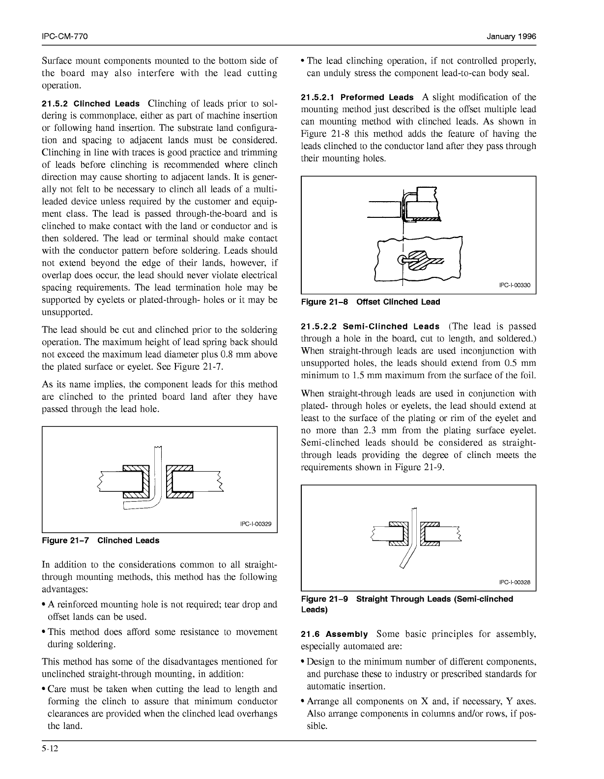
The lead should be cut and clinched prior to the soldering
operation. The maximum height of lead spring back should
not exceed the maximum lead diameter plus 0.8 mm above
the plated surface or eyelet. See Figure 21-7.
As its name implies, the component leads for this method
are clinched to the printed board land after they have
passed through the lead hole.
1
IPC-1-00329
Figure 21-7 Clinched Leads
In addition to the considerations common to all straight-
through mounting methods, this method has the following
advantages:
A reinforced mounting hole is not required; tear drop and
offset lands can be used.
This method does afford some resistance to movement
during soldering.
This method has some of the disadvantages mentioned for
unclinched straight-through mounting, in addition:
Care must be taken when cutting the lead to length and
forming the clinch to assure that minimum conductor
clearances are provided when the clinched lead overhangs
the land.
The lead clinching operation, if not controlled properly,
can unduly stress the component lead-to-can body seal.
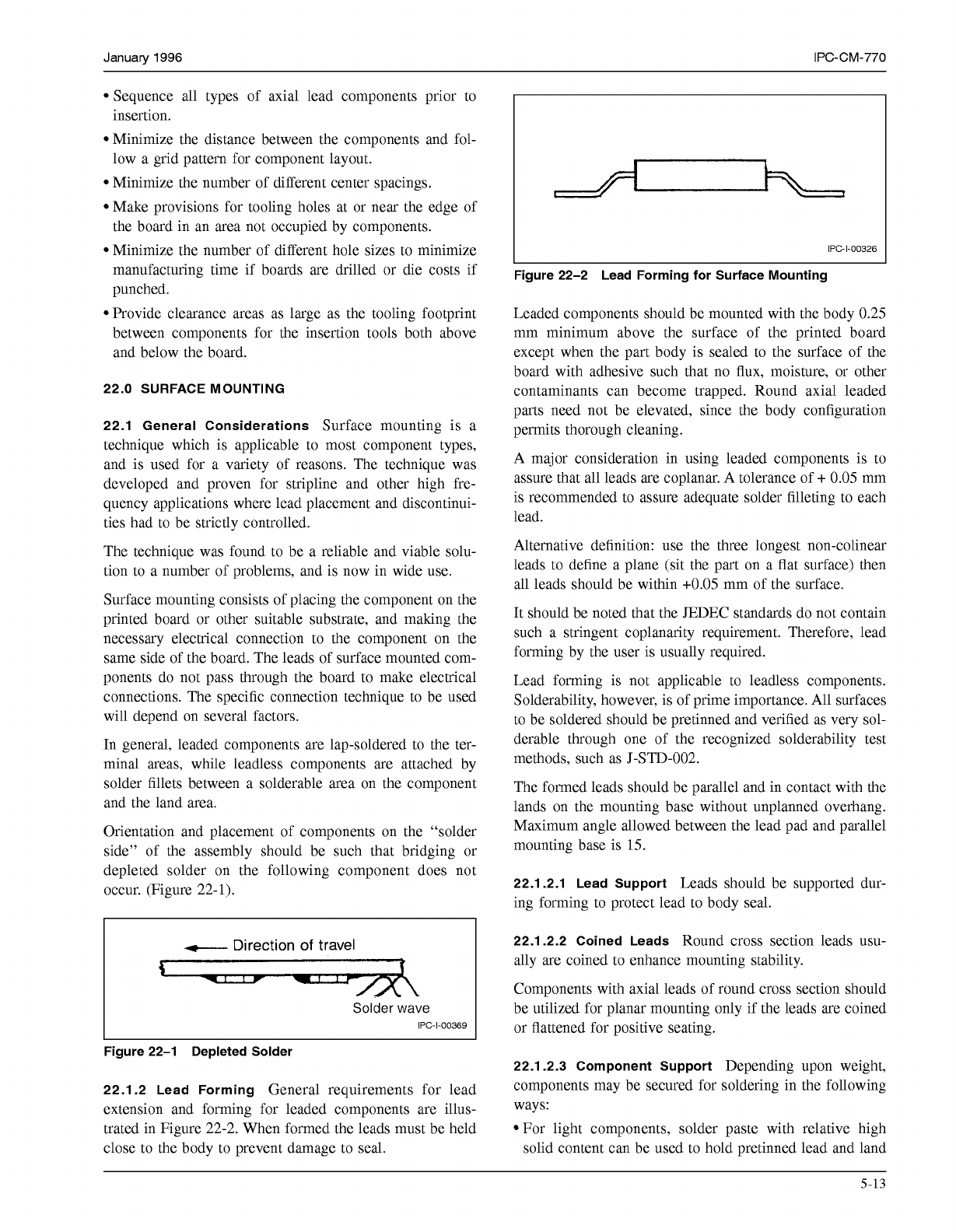
21 5.2.1 Preformed Leads
A slight modification of the
mounting method just described is the offset multiple lead
can mounting method with clinched leads. As shown in
Figure 21-8 this method adds the feature of having the
leads clinched to the conductor land after they pass through
their mounting holes.
m
IPC-1-00330
Figure 21-8 Offset Clinched Lead
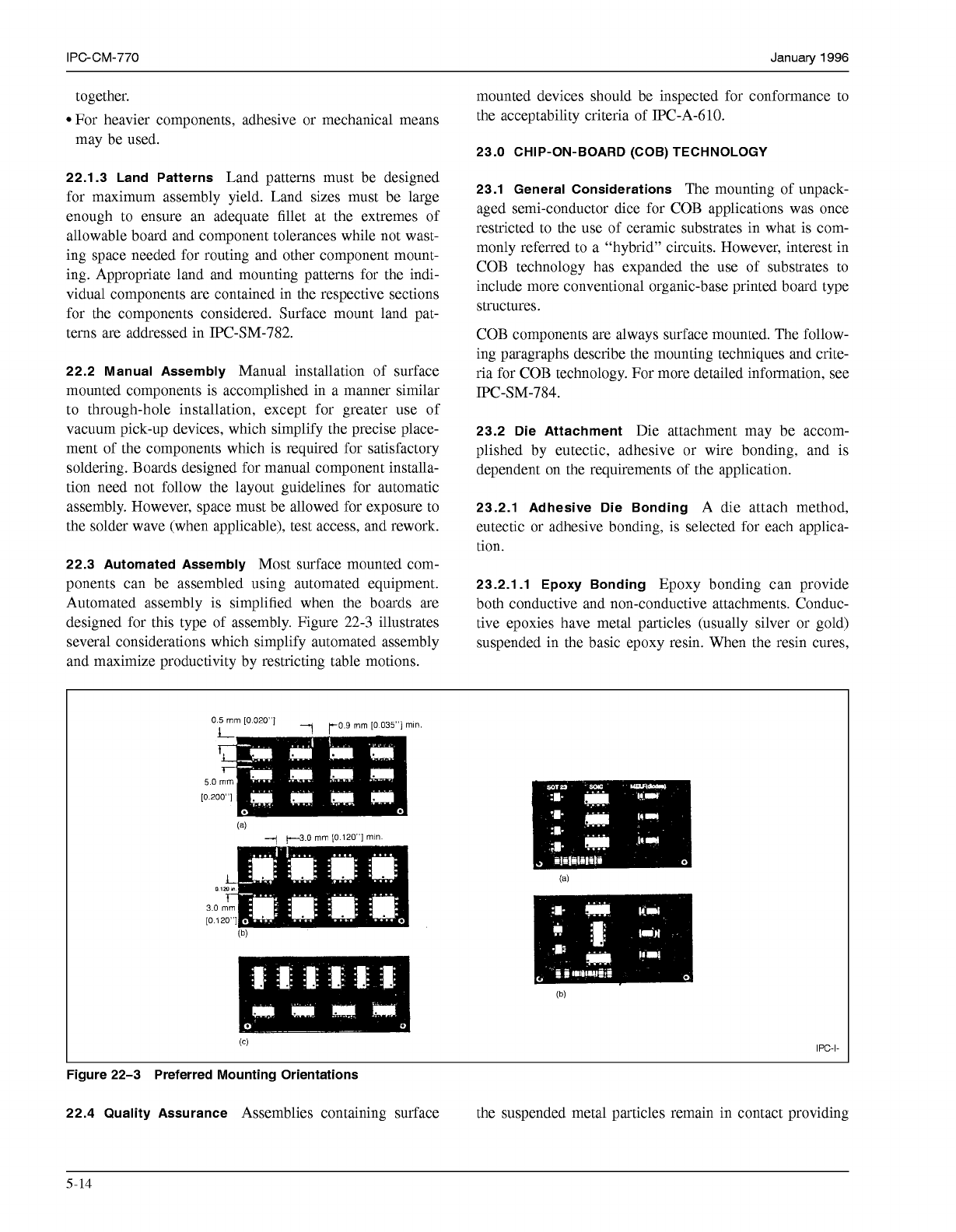
21.5.2.2 Semi-Clinched Leads
(The lead is passed
through a hole in the board, cut to length, and soldered.)
When straight-through leads are used inconjunction with
unsupported holes, the leads should extend from
0.5
mm
minimum to
1.5
mm maximum from the surface of the foil.
When straight-through leads are used in conjunction with
plated- through holes or eyelets, the lead should extend at
least to the surface of the plating or rim of the eyelet and
no more than 2.3 mm from the plating surface eyelet.
Semi-clinched leads should be considered as straight-
through leads providing the degree of clinch meets the
requirements shown in Figure 21-9.
n
a!
ID
IPC-1-00328
Figure 21-9 Straight Through Leads (Semi-clinched
Leads)
21.6 Assembly
Some basic principles for assembly,
especially automated are:
Design to the minimum number of different components,
and purchase these to industry or prescribed standards for
automatic insertion.
Arrange all components on
X
and, if necessary,
Y
axes.
Also arrange components in columns andor rows, if pos-
sible.
5-12
COPYRIGHT Association Connecting Electronics Industries
Licensed by Information Handling Services
COPYRIGHT Association Connecting Electronics Industries
Licensed by Information Handling Services
January
1996
IPC-CM-770
Sequence all types of axial lead components prior to
insertion.
Minimize the distance between the components and fol-
low a grid pattern for component layout.
Minimize the number of different center spacings.
Make provisions for tooling holes at or near the edge of
the board in an area not occupied by components.
Minimize the number of different hole sizes to minimize
manufacturing time if boards are drilled or die costs if
punched.
Provide clearance areas as large as the tooling footprint
between components for the insertion tools both above
and below the board.
22.0 SURFACE MOUNTING
22.1 General Considerations
Surface mounting is a
technique which is applicable to most component types,
and is used for a variety of reasons. The technique was
developed and proven for stripline and other high fre-
quency applications where lead placement and discontinui-
ties had to be strictly controlled.
The technique was found to be a reliable and viable solu-
tion to a number of problems, and is now in wide use.
Surface mounting consists of placing the component on the
printed board or other suitable substrate, and making the
necessary electrical connection to the component on the
same side of the board. The leads of surface mounted com-
ponents do not pass through the board to make electrical
connections. The specific connection technique to be used
will depend on several factors.
In general, leaded components are lap-soldered to the ter-
minal areas, while leadless components are attached by
solder fillets between a solderable area on the component
and the land area.
Orientation and placement of components on the “solder
side” of the assembly should be such that bridging or
depleted solder on the following component does not
occur. (Figure
22-
1).
f-
Direction
of
travel
F
Solder
wave
IPC-1-00369
Figure 22-1 Depleted Solder
22.1.2 Lead Forming
General requirements for lead
extension and forming for leaded components are illus-
trated in Figure
22-2.
When formed the leads must be held
close to the body to prevent damage to seal.
IPC-1-00326
Figure 22-2 Lead Forming for Surface Mounting
Leaded components should be mounted with the body
0.25
mm minimum above the surface of the printed board
except when the part body is sealed to the surface of the
board with adhesive such that no flux, moisture, or other
contaminants can become trapped. Round axial leaded
parts need not be elevated, since the body configuration
permits thorough cleaning.
A major consideration in using leaded components is to
assure that all leads are coplanar. A tolerance of
+
0.05
mm
is recommended to assure adequate solder filleting to each
lead.
Alternative definition: use the three longest non-colinear
leads to define a plane (sit the part on a flat surface) then
all leads should be within
+0.05
mm of the surface.
It should be noted that the JEDEC standards do not contain
such a stringent coplanarity requirement. Therefore, lead
forming by the user is usually required.
Lead forming is not applicable to leadless components.
Solderability, however, is of prime importance. All surfaces
to be soldered should be pretinned and verified as very sol-
derable through one of the recognized solderability test
methods, such as
J-STD-002.
The formed leads should be parallel and in contact with the
lands on the mounting base without unplanned overhang.
Maximum angle allowed between the lead pad and parallel
mounting base is
15.
22.1.2.1 Lead Support
Leads should be supported dur-
ing forming to protect lead to body seal.
22.1.2.2 Coined Leads
Round cross section leads usu-
ally are coined to enhance mounting stability.
Components with axial leads of round cross section should
be utilized for planar mounting only if the leads are coined
or flattened for positive seating.
22.1.2.3 Component Support
Depending upon weight,
components may be secured for soldering in the following
ways:
For light components, solder paste with relative high
solid content can be used to hold pretinned lead and land
5-13
COPYRIGHT Association Connecting Electronics Industries
Licensed by Information Handling Services
COPYRIGHT Association Connecting Electronics Industries
Licensed by Information Handling Services
IPC-CM-770
Januaty
1996
together.
For heavier components, adhesive or mechanical means
may be used.
22.1.3 Land Patterns
Land patterns must be designed
for maximum assembly yield. Land sizes must be large
enough to ensure an adequate fillet at the extremes of
allowable board and component tolerances while not wast-
ing space needed for routing and other component mount-
ing. Appropriate land and mounting patterns for the indi-
vidual components are contained in the respective sections
for the components considered. Surface mount land pat-
terns are addressed in IPC-SM-782.
22.2 Manual Assembly
Manual installation of surface
mounted components is accomplished in a manner similar
to through-hole installation, except for greater use
of
vacuum pick-up devices, which simplify the precise place-
ment of the components which is required for satisfactory
soldering. Boards designed for manual component installa-
tion need not follow the layout guidelines for automatic
assembly. However, space must be allowed for exposure to
the solder wave (when applicable), test access, and rework.
22.3 Automated Assembly
Most surface mounted com-
ponents can be assembled using automated equipment.
Automated assembly is simplified when the boards are
designed for this type of assembly. Figure 22-3 illustrates
several considerations which simplify automated assembly
and maximize productivity by restricting table motions.
mounted devices should be inspected for conformance to
the acceptability criteria of IPC-A-610.
23.0 CHIP-ON-BOARD (COB) TECHNOLOGY
23.1 General Considerations
The mounting of unpack-
aged semi-conductor dice for COB applications was once
restricted to the use of ceramic substrates in what is com-
monly referred to a "hybrid" circuits. However, interest in
COB technology has expanded the use of substrates to
include more conventional organic-base printed board type
structures.
COB components are always surface mounted. The follow-
ing paragraphs describe the mounting techniques and crite-
ria for COB technology. For more detailed information, see
IPC-SM-784.
23.2 Die Attachment
Die attachment may be accom-
plished by eutectic, adhesive or wire bonding, and is
dependent on the requirements of the application.
23.2.1 Adhesive Die Bonding
A die attach method,
eutectic or adhesive bonding, is selected for each applica-
tion.
23.2.1.1 Epoxy Bonding
Epoxy bonding can provide
both conductive and non-conductive attachments. Conduc-
tive epoxies have metal particles (usually silver or gold)
suspended in the basic epoxy resin. When the resin cures,
0.5
mm
[O
OZO"]
I
7
r0
9
mm
[O
035"l
mln.
Figure 22-3 Preferred Mounting Orientations
22.4 Quality Assurance
Assemblies containing surface the suspended metal particles remain in contact providing
5-14
COPYRIGHT Association Connecting Electronics Industries
Licensed by Information Handling Services
COPYRIGHT Association Connecting Electronics Industries
Licensed by Information Handling Services