IPC-CM-770D-1996.pdf - 第126页
IPC-CM-770 Januaty 1996 1 Layer 0.061 mm [O.O024"l Copper PATTERM IN COPPER FORMED """ "-"""" 2 Laver 0.036 mm [O.O014"l Copper -7 PATTERNS N CUPPER FORMED 7 IMAGE -IN0 0…
January
1996
IPC-CM-770
The bumping process is typically performed at the water
level. Water bumping may be performed by the semi-
conductor manufacturer, independent bumping facilities, or
by electronic companies producing “in-house” TAB Chip-
On-Tape components.
Since TAB technology is relatively new, bumped wafers
from semi-conductor manufacturers are not readily avail-
able. In addition, bare wafers may be difficult to obtain (for
bumping) because of the manufacturer’s concerns over pro-
cess propriety and subsequent bumping technology. As
TAB technology matures, these problems will probably be
resolved.
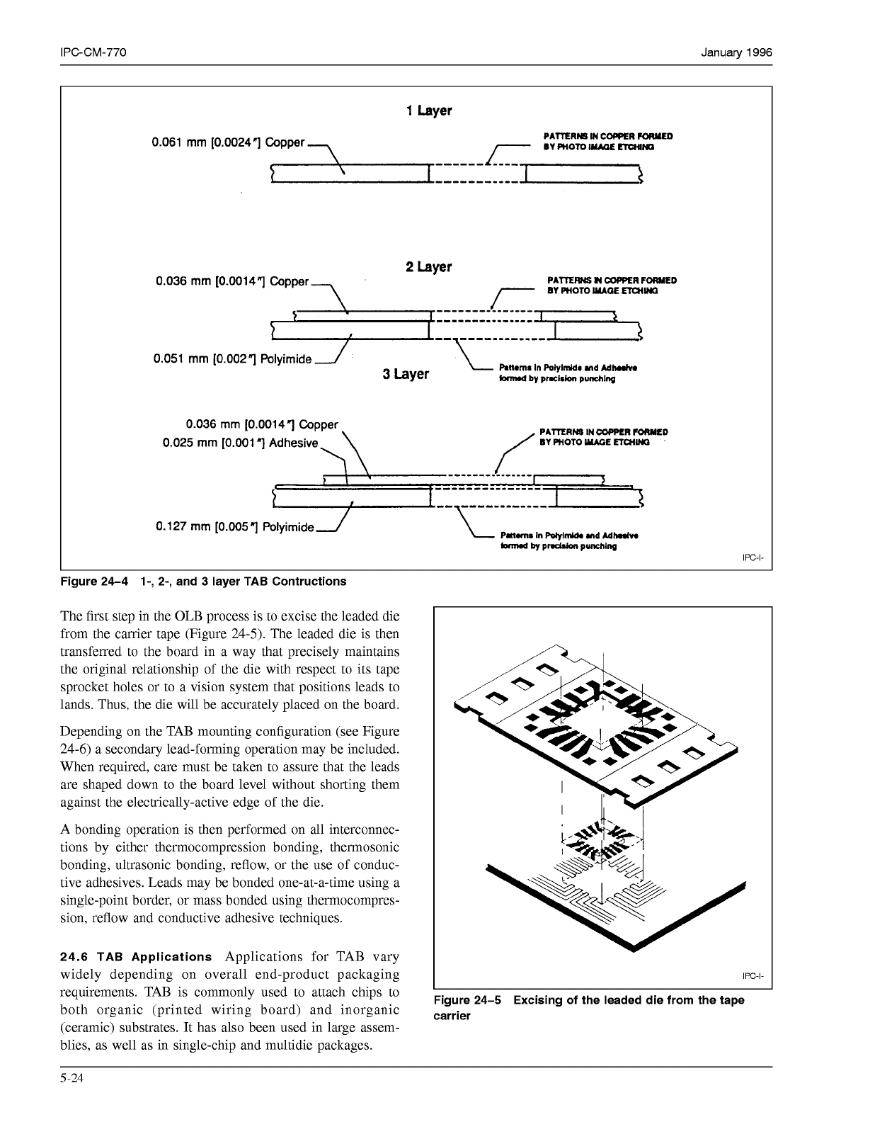
Bumps on the die are electroplated onto the barrier metal
at each land position. When the bump barrier metal passi-
vation overlaps the passivation, this completely seals the
die and further enhances TAB’S reliability as an assembly
process. Solder bumps, copper bumps and other metals can
also be used, and both copper and gold can be tin plated.
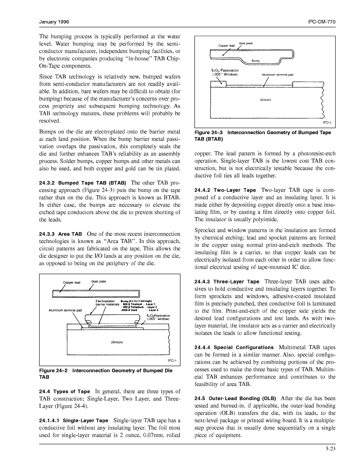
24.3.2 Bumped Tape TAB (BTAB)
The other TAB pro-
cessing approach (Figure 24-3) puts the bump on the tape
rather than on the die. This approach is known as BTAB.
In either case, the bumps are necessary to elevate the
etched tape conductors above the die to prevent shorting of
the leads.
24.3.3 Area TAB
One of the most recent interconnection
technologies is known as “Area TAB”. In this approach,
circuit patterns are fabricated on the tape. This allows the
die designer to put the I/O lands at any position on the die,
as opposed to being on the periphery of the die.
(
003’
wlndow)
(Slllcon)
IPC-I-
L
Figure 24-2 Interconnection Geometry of Bumped Die
TAB
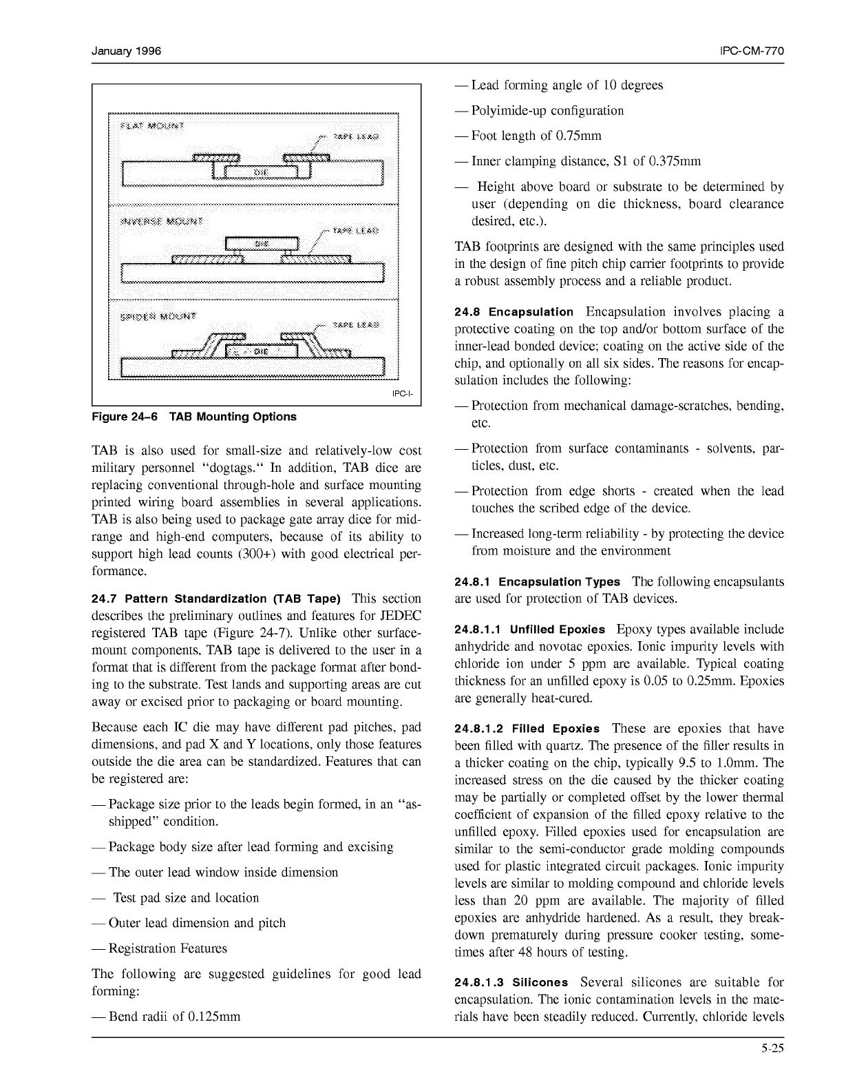
24.4 Types of Tape
In general, there are three types of
TAB construction; Single-Layer, Two Layer, and Three-
Layer (Figure 24-4).
24.1.4.1 Single-Layer Tape
Single-layer TAB tape has a
conductive foil without any insulating layer. The foil most
used for single-layer material is 2 ounce, 0.07mm, rolled
Capper lead
Gold plate
/
Bump
S1O2
Passlvatlon
(005”
Window)
7
Alumlnum
lermlnal pad
(Slllcon)
IPC-I-
Figure 24-3 Interconnection Geometry of Bumped Tape
TAB (BTAB)
copper. The lead pattern is formed by a photoresist-etch
operation. Single-layer TAB is the lowest cost TAB con-
struction, but is not electrically testable because the con-
ductive foil ties all leads together.
24.4.2 Two-Layer Tape
Two-layer TAB tape is com-
posed of a conductive layer and an insulating layer. It is
made either by depositing copper directly onto a base insu-
lating film, or by casting a film directly onto copper foil.
The insulator is usually polyimide.
Sprocket and window patterns in the insulation are formed
by chemical etching; lead and spocket patterns are formed
in the copper using normal print-and-etch methods. The
insulating film is a carrier,
so
that copper leads can be
electrically isolated from each other in order to allow func-
tional electrical testing of tape-mounted IC dice.
24.4.3 Three-Layer Tape
Three-layer TAB uses adhe-
sives to hold conductive and insulating layers together. To
form sprockets and windows, adhesive-coated insolated
film is precisely punched, then conductive foil is laminated
to the film. Print-and-etch of the copper side yields the
desired lead configurations and test lands. As with two-
layer material, the insulator acts as a carrier and electrically
isolates the leads to allow functional testing.
24.4.4 Special Configurations
Multimetal TAB tapes
can be formed in a similar manner. Also, special configu-
rations can be achieved by combining portions of the pro-
cesses used to make the three basic types of TAB. Multim-
eta1 TAB enhances performance and contributes to the
feasibility of area TAB.
24.5 Outer-Lead Bonding (OLB)
After the die has been
tested and burned-in, if applicable, the outer-lead bonding
operation (OLB) transfers the die, with its leads, to the
next-level package or printed wiring board. It is a multiple-
step process that is usually done sequentially on a single
piece of equipment.
5-23
COPYRIGHT Association Connecting Electronics Industries
Licensed by Information Handling Services
COPYRIGHT Association Connecting Electronics Industries
Licensed by Information Handling Services
IPC-CM-770
Januaty
1996
1
Layer
0.061 mm [O.O024"l
Copper
PATTERM
IN
COPPER
FORMED
"""
"-""""
2
Laver
0.036 mm [O.O014"l
Copper
-7
PATTERNS
N
CUPPER
FORMED
7
IMAGE
-IN0
0.051 mm
10.002
1
Polyimide
1
3
Layer
kmrd
by
pmcWon
punching
Rnm.
In
POlylmM~
and
MM
0.036 mm
[0.00141
Copper
0.025
mm
[0.001
Adhesive
3-
"""""""_
"""""""_
"\
""""""
0.127 mm
[0.0057
Polyimide~
IPC-I-
Figure 24-4 1-, 2-, and
3
layer TAB Contructions
The first step in the OLB process is to excise the leaded die
from the carrier tape (Figure 24-5). The leaded die is then
transferred to the board in a way that precisely maintains
the original relationship of the die with respect to its tape
sprocket holes or to a vision system that positions leads to
lands. Thus, the die will be accurately placed on the board.
Depending on the TAB mounting configuration (see Figure
24-6) a secondary lead-forming operation may be included.
When required, care must be taken to assure that the leads
are shaped down to the board level without shorting them
against the electrically-active edge of the die.
A bonding operation is then performed on all interconnec-
tions by either thermocompression bonding, thermosonic
bonding, ultrasonic bonding, reflow, or the use of conduc-
tive adhesives. Leads may be bonded one-at-a-time using a
single-point border, or mass bonded using thermocompres-
sion, reflow and conductive adhesive techniques.
24.6 TAB Applications
Applications for TAB vary
widely depending on overall end-product packaging
IPC-I-
requirements. TAB is commonly used to attach chips to
Figure
24-5
Excising
of
the
leaded die
from
the
tape
both organic (printed wiring board) and inorganic
carrier
(ceramic) substrates. It has also been used in large assem-
blies, as well as in single-chip and multidie packages.
L
5-24
COPYRIGHT Association Connecting Electronics Industries
Licensed by Information Handling Services
COPYRIGHT Association Connecting Electronics Industries
Licensed by Information Handling Services
January
1996
IPC-CM-770
...........................................................................
.........
”...
....
”.%.”%
....-.-..-
.
.”
t
IPC-I-
I
L
Figure 24-6 TAB Mounting Options
TAB is also used for small-size and relatively-low cost
military personnel “dogtags.“ In addition, TAB dice are
replacing conventional through-hole and surface mounting
printed wiring board assemblies in several applications.
TAB is also being used to package gate array dice for mid-
range and high-end computers, because of its ability to
support high lead counts (300+) with good electrical per-
formance.
24.7 Pattern Standardization (TAB Tape)
This section
describes the preliminary outlines and features for JEDEC
registered TAB tape (Figure 24-7). Unlike other surface-
mount components, TAB tape is delivered to the user in a
format that is different from the package format after bond-
ing to the substrate. Test lands and supporting areas are cut
away or excised prior to packaging or board mounting.
Because each IC die may have different pad pitches, pad
dimensions, and pad
X
and
Y
locations, only those features
outside the die area can be standardized. Features that can
be registered are:
-
Package size prior to the leads begin formed, in an “as-
shipped” condition.
-
Package body size after lead forming and excising
-
The outer lead window inside dimension
-
Test pad size and location
-
Outer lead dimension and pitch
-
Registration Features
The following are suggested guidelines for good lead
forming:
-Bend radii of 0.125mm
-
Lead forming angle of
10
degrees
-
Polyimide-up configuration
-
Foot length of 0.75mm
-
Inner clamping distance,
S
1
of 0.375mm
-
Height above board or substrate to be determined by
user (depending on die thickness, board clearance
desired, etc.).
TAB footprints are designed with the same principles used
in the design of fine pitch chip carrier footprints to provide
a robust assembly process and a reliable product.
24.8 Encapsulation
Encapsulation involves placing a
protective coating on the top and/or bottom surface of the
inner-lead bonded device; coating on the active side of the
chip, and optionally on all six sides. The reasons for encap-
sulation includes the following:
-
Protection from mechanical damage-scratches, bending,
etc.
-Protection from surface contaminants
-
solvents, par-
ticles, dust, etc.
-Protection from edge shorts
-
created when the lead
touches the scribed edge of the device.
-
Increased long-term reliability
-
by protecting the device
from moisture and the environment
24.8.1 Encapsulation Types
The following encapsulants
are used for protection of TAB devices.
24.8.1.1 Unfilled Epoxies
Epoxy types available include
anhydride and novotac epoxies. Ionic impurity levels with
chloride ion under
5
ppm are available. Typical coating
thickness for an unfilled epoxy is
0.05
to 0.25mm. Epoxies
are generally heat-cured.
24.8.1.2 Filled Epoxies
These are epoxies that have
been filled with quartz. The presence of the filler results in
a thicker coating on the chip, typically
9.5
to l.Omm. The
increased stress on the die caused by the thicker coating
may be partially or completed offset by the lower thermal
coefficient of expansion of the filled epoxy relative to the
unfilled epoxy. Filled epoxies used for encapsulation are
similar to the semi-conductor grade molding compounds
used for plastic integrated circuit packages. Ionic impurity
levels are similar to molding compound and chloride levels
less than 20 ppm are available. The majority of filled
epoxies are anhydride hardened. As a result, they break-
down prematurely during pressure cooker testing, some-
times after 48 hours of testing.
24.8.1.3 Silicones
Several silicones are suitable for
encapsulation. The ionic contamination levels in the mate-
rials have been steadily reduced. Currently, chloride levels
5-25
COPYRIGHT Association Connecting Electronics Industries
Licensed by Information Handling Services
COPYRIGHT Association Connecting Electronics Industries
Licensed by Information Handling Services