IPC-CM-770D-1996.pdf - 第127页
January 1996 IPC-CM-770 ........................................................................... ......... ”... .... ”.%.”% ....-.-..- . .” t IPC-I- I L Figure 24-6 TAB Mounting Options TAB is also used for small-size…
IPC-CM-770
Januaty
1996
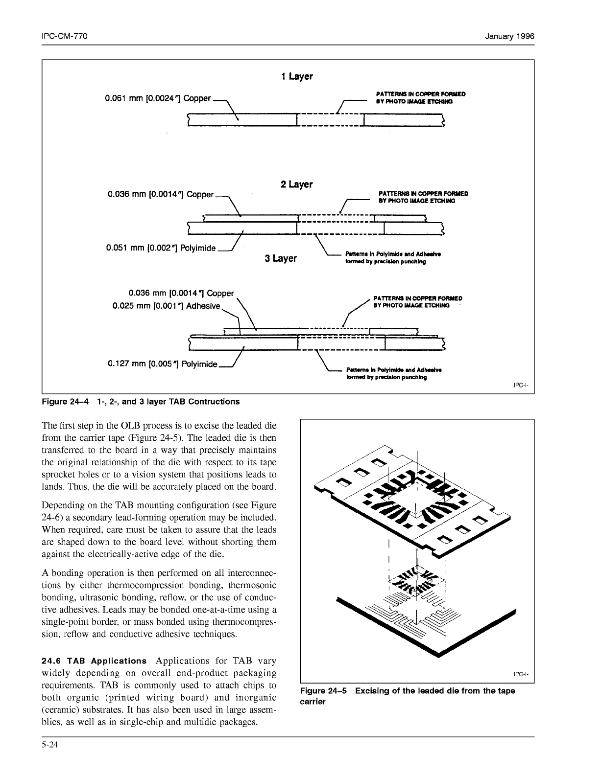
1
Layer
0.061 mm [O.O024"l
Copper
PATTERM
IN
COPPER
FORMED
"""
"-""""
2
Laver
0.036 mm [O.O014"l
Copper
-7
PATTERNS
N
CUPPER
FORMED
7
IMAGE
-IN0
0.051 mm
10.002
1
Polyimide
1
3
Layer
kmrd
by
pmcWon
punching
Rnm.
In
POlylmM~
and
MM
0.036 mm
[0.00141
Copper
0.025
mm
[0.001
Adhesive
3-
"""""""_
"""""""_
"\
""""""
0.127 mm
[0.0057
Polyimide~
IPC-I-
Figure 24-4 1-, 2-, and
3
layer TAB Contructions
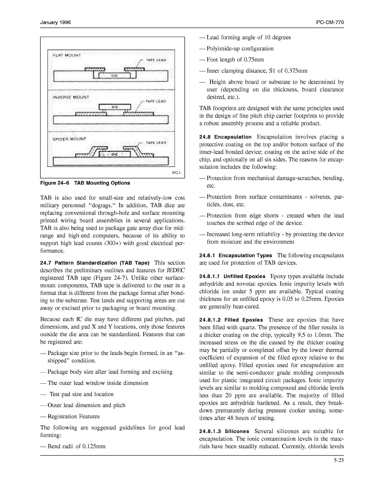
The first step in the OLB process is to excise the leaded die
from the carrier tape (Figure 24-5). The leaded die is then
transferred to the board in a way that precisely maintains
the original relationship of the die with respect to its tape
sprocket holes or to a vision system that positions leads to
lands. Thus, the die will be accurately placed on the board.
Depending on the TAB mounting configuration (see Figure
24-6) a secondary lead-forming operation may be included.
When required, care must be taken to assure that the leads
are shaped down to the board level without shorting them
against the electrically-active edge of the die.
A bonding operation is then performed on all interconnec-
tions by either thermocompression bonding, thermosonic
bonding, ultrasonic bonding, reflow, or the use of conduc-
tive adhesives. Leads may be bonded one-at-a-time using a
single-point border, or mass bonded using thermocompres-
sion, reflow and conductive adhesive techniques.
24.6 TAB Applications
Applications for TAB vary
widely depending on overall end-product packaging
IPC-I-
requirements. TAB is commonly used to attach chips to
Figure
24-5
Excising
of
the
leaded die
from
the
tape
both organic (printed wiring board) and inorganic
carrier
(ceramic) substrates. It has also been used in large assem-
blies, as well as in single-chip and multidie packages.
L
5-24
COPYRIGHT Association Connecting Electronics Industries
Licensed by Information Handling Services
COPYRIGHT Association Connecting Electronics Industries
Licensed by Information Handling Services
January
1996
IPC-CM-770
...........................................................................
.........
”...
....
”.%.”%
....-.-..-
.
.”
t
IPC-I-
I
L
Figure 24-6 TAB Mounting Options
TAB is also used for small-size and relatively-low cost
military personnel “dogtags.“ In addition, TAB dice are
replacing conventional through-hole and surface mounting
printed wiring board assemblies in several applications.
TAB is also being used to package gate array dice for mid-
range and high-end computers, because of its ability to
support high lead counts (300+) with good electrical per-
formance.
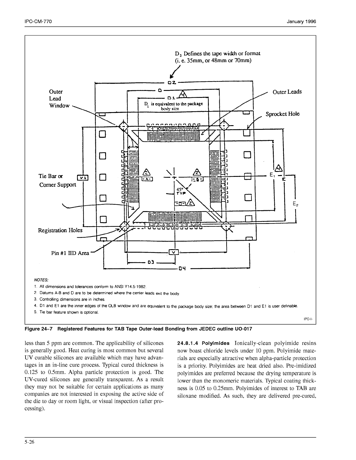
24.7 Pattern Standardization (TAB Tape)
This section
describes the preliminary outlines and features for JEDEC
registered TAB tape (Figure 24-7). Unlike other surface-
mount components, TAB tape is delivered to the user in a
format that is different from the package format after bond-
ing to the substrate. Test lands and supporting areas are cut
away or excised prior to packaging or board mounting.
Because each IC die may have different pad pitches, pad
dimensions, and pad
X
and
Y
locations, only those features
outside the die area can be standardized. Features that can
be registered are:
-
Package size prior to the leads begin formed, in an “as-
shipped” condition.
-
Package body size after lead forming and excising
-
The outer lead window inside dimension
-
Test pad size and location
-
Outer lead dimension and pitch
-
Registration Features
The following are suggested guidelines for good lead
forming:
-Bend radii of 0.125mm
-
Lead forming angle of
10
degrees
-
Polyimide-up configuration
-
Foot length of 0.75mm
-
Inner clamping distance,
S
1
of 0.375mm
-
Height above board or substrate to be determined by
user (depending on die thickness, board clearance
desired, etc.).
TAB footprints are designed with the same principles used
in the design of fine pitch chip carrier footprints to provide
a robust assembly process and a reliable product.
24.8 Encapsulation
Encapsulation involves placing a
protective coating on the top and/or bottom surface of the
inner-lead bonded device; coating on the active side of the
chip, and optionally on all six sides. The reasons for encap-
sulation includes the following:
-
Protection from mechanical damage-scratches, bending,
etc.
-Protection from surface contaminants
-
solvents, par-
ticles, dust, etc.
-Protection from edge shorts
-
created when the lead
touches the scribed edge of the device.
-
Increased long-term reliability
-
by protecting the device
from moisture and the environment
24.8.1 Encapsulation Types
The following encapsulants
are used for protection of TAB devices.
24.8.1.1 Unfilled Epoxies
Epoxy types available include
anhydride and novotac epoxies. Ionic impurity levels with
chloride ion under
5
ppm are available. Typical coating
thickness for an unfilled epoxy is
0.05
to 0.25mm. Epoxies
are generally heat-cured.
24.8.1.2 Filled Epoxies
These are epoxies that have
been filled with quartz. The presence of the filler results in
a thicker coating on the chip, typically
9.5
to l.Omm. The
increased stress on the die caused by the thicker coating
may be partially or completed offset by the lower thermal
coefficient of expansion of the filled epoxy relative to the
unfilled epoxy. Filled epoxies used for encapsulation are
similar to the semi-conductor grade molding compounds
used for plastic integrated circuit packages. Ionic impurity
levels are similar to molding compound and chloride levels
less than 20 ppm are available. The majority of filled
epoxies are anhydride hardened. As a result, they break-
down prematurely during pressure cooker testing, some-
times after 48 hours of testing.
24.8.1.3 Silicones
Several silicones are suitable for
encapsulation. The ionic contamination levels in the mate-
rials have been steadily reduced. Currently, chloride levels
5-25
COPYRIGHT Association Connecting Electronics Industries
Licensed by Information Handling Services
COPYRIGHT Association Connecting Electronics Industries
Licensed by Information Handling Services
IPC-CM-770
Januaty
1996
D,
Defines
the
tape
width
or
format
(i.
e.
35mm,
or
48mm
or
70mm)
J
I
OZ
i
Pin
#1
IID
Area
NOTES:
1
All dimensions and tolerances conform
to
ANSI
Y14.5-1982
2
Datums A-B and
D
are
to
be determined where the center leads exlt the
body
3.
Contrdlmg dimensions are in inches.
4. D1
and
El
are the inner edges
of
the OLB
window
and are equlvaknt
to
the package
body
size: the area between
Dl
and
El
is user delInable.
5.
Tie
bar
feature shown
IS
opttonal.
IPC-I-
Figure
24-7
Registered Features for TAB Tape Outer-lead Bonding from
JEDEC
outline
UO-O17
less than
5
ppm are common. The applicability of silicones
is generally good. Heat curing is most common but several
UV curable silicones are available which may have advan-
tages in an in-line cure process. Typical cured thickness is
0.125 to 0.5mm. Alpha particle protection is good. The
UV-cured silicones are generally transparent. As a result
they may not be suitable for certain applications as many
companies are not interested in exposing the active side
of
the die to day or room light, or visual inspection (after pro-
cessing).
24.8.1.4 Polyimides
Ionically-clean polyimide resins
now boast chloride levels under
10
ppm. Polyimide mate-
rials are especially attractive when alpha-particle protection
is a priority. Polyimides are heat dried also. Pre-imidized
polyimides are preferred because the drying temperature is
lower than the monomeric materials. Typical coating thick-
ness is
0.05
to 0.25mm. Polyimides of interest to TAB are
siloxane modified. As such, they are delivered pre-cured,
5-26
COPYRIGHT Association Connecting Electronics Industries
Licensed by Information Handling Services
COPYRIGHT Association Connecting Electronics Industries
Licensed by Information Handling Services