SIPLACE 80 F4_EN.pdf - 第29页
28 Description The Flip Ch ip component vision module extend s the c apability of processing Fine Pitch and Fl ip Chip components with extreme fine lead pitches. T his add-on modu le for the Fine Pitch component v i- sio…

27
Description
The Fine Pitch component vision
module operates according to a
sophisticated lighting technology
and utilizes diverse analysis algo-
rithms. Despite the great diversity
of components it boasts a very
high recognition reliability with all
SMD modules. Like all other vision
modules, this one is also con-
nected to the station’s vision
processor.
The components are illuminated
from three lighting planes whose
intensity can be adjusted in 256
increments. This enables an opti-
mal illumination of each compo-
nent. The gray-scale picture re-
corded is analyzed on the basis of
the algorithm best suited for the
package form.
ICs, Flip Chips and IC-sockets are
centered on the basis over the
leads or bumps. In the case of
chips, bare chips for subsequent
wire bonding and odd-shaped
components, centering is based
on the outside contour (outline
measurement).
A special inspection mode for the
critical IC lead ends (HALE) pre-
cisely determines the lateral lead
bend as well as pitch error and
lead offset. This greatly reduces
the risk of short circuits.
Beyond this, the rotational angle
deviation and the X-/Y-offset of the
component relative to the nozzle
center is ascertained and factored
in during placement. The X-/Y-
offset also results in the correction
of the pick-up position.
In order to have the vision module
center a component which it does
not yet know, it must first be de-
scribed geometrically in the pack-
age form (GF) file. The component
test makes it possible to check at
the station to determine whether
adjustments, in lighting for exam-
ple, are necessary. These adjust-
ments are automatically assigned
as a file to the pertinent package
form which represents a compo-
nent type. Hence they are valid for
all of the stations in a line. As the
final step, the GF number of the
component type is entered in the
component file.
Vision Sensor Technology:
Fine Pitch Component Vision Module for the
Pick & Place Head
Technical Data
Max. component size
32 x 32 mm (single measurement)
55 x 55 mm* (multiple measurement)
Component range
PLCC, LCCC, QFP, SO, BGA, Flip Chip
components with connections up to
55 x 55 mm (J-leads and gull-wings,
balls, bumps)
Camera’s field of view 38 x 38 mm
Illumination
Front light
(3 freely programmable planes)
Analysis algorithms Compare page 25
* Larger components available on request

28
Description
The Flip Chip component vision
module extends the capability of
processing Fine Pitch and Flip Chip
components with extreme fine
lead pitches. This add-on module
for the Fine Pitch component vi-
sion module offers a far higher
resolution. The lighting layout is
fundamentally changed in the pro-
cess. At optimal illumination, the
imaging of the bumps is as large
as possible and the orthogonal dis-
ruptive structures (e.g., chip
printed conductor tracks) are sup-
pressed. In the event of less pro-
nounced disruptive structures, the
intensity can be increased by
combined lighting. This results in a
high recognition reliability even
with usually square surfaces of
bumped Flip Chips in the conduc-
tive adhesive technology.
Special search algorithms are used
to recognize the bumps (balls) in
surroundings where fault condi-
tions usually prevail.
Vision Sensor Technology:
Flip Chip Component Vision Module for the
Pick & Place Head (Option)
Technical Data
Flip Chip size
with single measurement
with multiple measurement
1 x 1 mm
up to max. 7 x 9 mm
max. 20 x 20 mm
Dimensions < 3 x 6 mm
Special nozzle,
feeding tolerance < 0.2 mm edge length
Min. bump diameter 80 µm
Placement cycle
min. 2 s
(depending on number of bumps)
IC-pitch:
Lead pitch
Bump pitch
0.25 mm
0.15 mm
Camera’s field of view 9 x 11.5 mm
Illumination
Front light
(3 freely programmable planes)
29
Description
The optional coplanarity check fur-
ther enhances placement reliabil-
ity. This check is always con-
ducted right after the deviation of
position is ascertained with the
Fine Pitch vision module of the
Pick & Place head.
The coplanarity module is installed
next to the PCB conveyor along
with the Fine Pitch vision module
of the Pick & Place head.
One of the biggest problems in
Fine Pitch technology, the copla-
narity of leads, can be largely
eliminated by taking one additional
step during inspection. The copla-
narity module is employed to con-
duct a contactless, sequential ver-
tical scanning of the IC lead
structure on the basis of the laser
triangulation principle. The height
profile thus obtained for all of the
rows of leads is used to calculate
placement plane of the IC. The
programmed tolerance band based
on this placement plane then be-
comes effective.
If even one lead is outside this
placement area, the component is
excluded from the placement pro-
cess. It is gently placed back in the
Waffle Pack, entered on the repair
list and automatically repaired.
The component picked up by the
placement head may be crooked,
e.g., because one surface of the
package is not parallel to the row
of leads. The calculation of the
placement eliminates any influ-
ence this might have on
placement however.
As the result of extensive security
measures, the laser can only be
operated in the closed machine. It
then conforms to Safety Class 1
(not dangerous for eyes and skin).
Barring manipulation of the protec-
tive devices, the laser will not op-
erate outside the machine. Fol-
lowing impermissible tampering,
the laser complies with Class B.
On SIPLACE placement systems
the component which is picked up
is placed on the PCB immediately
after the coplanarity check. This
procedure ensures that no change
can occur after the check as the
result of any subsequent mechani-
cal influence. Unlike other designs,
with SIPLACE machines it is not
necessary to pick up the compo-
nent again or to transport it in a
special pick-up movement.
Vision Sensor Technology:
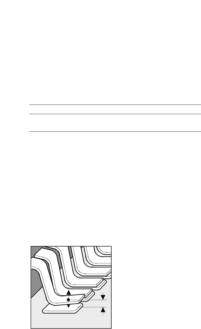
Coplanarity Module for the Pick & Place Head (Option)
Z
Effects of coplanarity (lateral ben-
ding of leads) of a populated com-
ponent
Accuracy of the coplanarity module
Uncertainty of checking in case of real components
Dimensions
U
99.73
[µm]*
32 x 32 mm
55 x 55 mm
21.5
22.7
* Checking uncertainty of a single measurement with a confidence interval of 99.73%
(corresponds to 3
σ
)