Test_Flow_for_Advanced_Packages_WhitePaper_1115.pdf - 第11页
ADV ANCED P ACKAGE TEST FLOW 1 1 References Huemoeller , R. (2015). “Silicon W afer Integrated Fan-out T echnology ,” – Chip Scale Review, April/May Issue Karim, N. (201 1). "2.5D/3D Package Si gnal Integrity - A Pa…
ADVANCED PACKAGE TEST FLOW 9
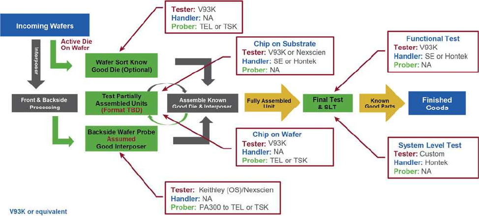
Universal Test Flow for Advanced Packages
Despite the differences of the build technique employed with SLIM, 2.5D or 3D, the test
flow in Figure 5 defines the universal test flow that can be taken when building such devices. The
test stages are green boxes, while the assembly / middle end of line (MEOL) processes are shown in
black. The incoming and outgoing from the OSAT are shown in blue. The red boxes define the test
equipment used at each stage with a description of the process or test stage.
Figure 5: Test Flow for Advanced Packages
Incoming wafers have two alternate test paths: active wafers are tested as full thickness
wafers and passive interposers with test structures are tested after thinning and mounting on a glass
carrier wafer. If the interposer wafer is tested on an automated prober with a wafer loader, care must
be taken to ensure the prober recognizes the notch on the wafer for orientation. During interposer
test, only the test structures’ connectivity is verified, and if found good, all interconnects on the
interposer die are assumed good.
ADVANCED PACKAGE TEST FLOW 10
Known good die and assumed good interposers are assembled and the partially assembled
unit is sent to test. Depending on the test criteria, the tests can be either opens/ shorts to verify
connectivity or functional tests to check for performance variations. When there are multiple dies on
a single chip, after each die is attached, the partially assembled unit is tested. The form factor at test
will depend on the assembly technique i.e., Chip on Substrate (CoS) or Chip on Wafer (CoW). In the
case of CoW, the material hander is a prober, while in the case of CoS, a final test handler is
employed. This process of partially assembled testing continues as new dies or devices are added to
the unit being built. In the case of CoS, the customer may request that the partially assembled unit be
tested on SLT.
After full assembly, the unit is tested using ATE and, in some cases, is sent to SLT. If the
device is equipped with non-volatile RAM, tracking information such as wafer number, lot number,
die x, y, etc. are written to the device during test, enabling unit level traceability. In some cases, the
device is marked with a 2D barcode that can be scanned to derive the unit level information.
Conclusions
Advanced packages that use SLIM/2.5D or 3D assembly techniques tend to pack high
performance while consuming lower power into a smaller and slimmer package. Each die in the
package in itself is a high performance unit. Integrating these individual dies into a single package
provides improved performance greater than the sum of the individual components if packaged
separately. With the addition of each individual die to the package, the cost of the package increases.
Therefore, it is absolutely necessary to test each individual die for performance prior to assembly
and test the partially assembled units during the assembly process to minimize scrap costs.
Furthermore, with appropriate analysis and package partitioning, each classification of package or
subassembly can be tested in a universal test flow to satisfy the most stringent criteria.

ADVANCED PACKAGE TEST FLOW 11
References
Huemoeller, R. (2015). “Silicon Wafer Integrated Fan-out Technology,” – Chip Scale Review,
April/May Issue
Karim, N. (2011). "2.5D/3D Package Signal Integrity - A Paradigm Shift," MEPTEC
Kelly, M. (2014). "2.5D TSV enablement of a multiple processor SiP," Chip Scale Review,
May/June Issue