Test_Flow_for_Advanced_Packages_WhitePaper_1115.pdf - 第4页
ADV ANCED P ACKAGE TEST FLOW 4 T est Flow for Advanced Packages (2.5D/SLIM/3D) The process of building a “chip” can be viewed as a fan-out process, where the die is attached to a substrate or interposer , which provide s…
ADVANCED PACKAGE TEST FLOW 3
Abstract
With the newest integrated circuit (IC) packages, the old adage of “faster, cheaper and better” (FCB)
gets an additional adjective - “slimmer.” This generates the new term “faster, cheaper, better &
slimmer” (FCBS) that should become a new industry buzzword. With FCB, it was a generally
accepted principle that one could get “two out of the three.” However, with the FCBS concept, it is
understood that the combined product will exhibit all four characteristics with combined benefits
that outweigh the sum of the individual components.
Product designers cognizant of the FCBS requirements are pushing outsourced assembly and
test (OSAT) companies to deliver integrated modules (chips) that do more, with a thinner form
factor. This includes integrating devices into a package, creating a System in Package (SiP), which
combines devices from different technology nodes. Such integration has been made possible by the
use of advanced substrates that provide fine line and space, or with the use of silicon interposers that
use Through Silicon Via (TSV) technology. Alternatively, product integrators can use Amkor’s most
advanced packaging solution, Silicon-Less Integrated Module (SLIM™) technology that eliminates
TSVs, further reducing package height. Die stacking technologies including 3D and package
stacking approaches such as Package-on-Package (PoP) are also employed to deliver FCBS
products.
One important aspect of achieving an FCBS product is reducing scrap cost. This is achieved
by an interactive test flow, wherein the device (system/ sub-system) being built is tested as
individual components as well as tested during the assembly process. Testing partially assembled
devices poses new challenges and risks, such as handling thinned dies and exposed pads. This paper
examines the various test insert points and proposes a suitable test flow for products that use
advanced packaging technologies.
ADVANCED PACKAGE TEST FLOW 4
Test Flow for Advanced Packages (2.5D/SLIM/3D)
The process of building a “chip” can be viewed as a fan-out process, where the die is
attached to a substrate or interposer, which provides electrical connectivity from the enclosed die to
the outside world. The substrate converts the die’s fine pitch and small pads to a pad size and pitch
that can be easily assembled on a printed circuit board. In the case of a multichip module, the
substrate or interposer also provides electrical connectivity to other dies on the interposer or
substrate. Typically the substrates are electrically tested by the substrate manufacturer and only
known good substrates (KGSu) are shipped to the OSAT. In the case of a 2.5D interposer, since the
interposers are shipped to the OSAT as full thickness wafers, top to bottom connections on the
interposer can only be checked after the wafer is thinned and TSVs are exposed. In the case of 3D
chips, known good die (KGD) are stacked and bonded over each other. However, in the case of SiPs,
either KGD or known good devices are populated onto the substrate or interposer.
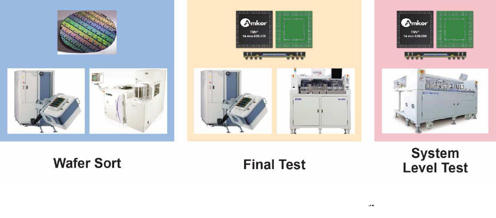
Figure 1: Traditional Test Insertion Points for Semiconductor Test
As shown in Figure 1, the standard test insertion points during traditional semiconductor test
at an OSAT are Wafer Sort (WS), Final Test (FT) and, in some cases, System Level Test (SLT). At
Wafer Sort, OSAT’s use automated test equipment (ATE) and automated probers that handle full
thickness wafers (~800 µm). Here devices are tested for functionality rather than performance. After
ADVANCED PACKAGE TEST FLOW 5
all the assembly is completed and the device is in its final form, the device is sent for FT. During FT,
the device is tested for performance using the minimum datasheet specifications as the lower limit.
Devices that are targeted for specific applications in a reference design environment undergo SLT.
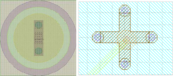
Improving Interposer Yield using Redundancy - Eliminating the Need to Test
The interposer wafer may consist of two or three metal layers, usually built using mature
process node technologies such as 90nm or 65nm. These proven technologies provide highly reliable
connections between dies and from die to the TSVs. The potential risk in connectivity can occur if
the interposer has non-uniform TSVs. For example, if a single TSV were used to make a connection
between the front side metal and the backside C4, and if this TSV’s height were 10 µm shorter than
the rest, no connection would result. However, adding multiple (one or more) redundant TSVs for
each C4 connection, as shown in Figure 2, significantly increases the yield to the point where testing
may not be necessary.
If a customer deems interposer testing necessary, they add daisy chain structures at certain
strategic locations. Testing is usually done from the C4 side, where the pad diameter is 80 µm and
the pitch is 120 to 150 µm, allowing for simple cantilever probe cards for test. During interposer test,
if an open is detected in any of these test structures, the interposer die is marked as bad (unusable).
Figure 2: Redundant TSVs to C4 connection