Test_Flow_for_Advanced_Packages_WhitePaper_1115.pdf - 第6页
ADV ANCED P ACKAGE TEST FLOW 6 T est Challenges with Advanced Packaging T echnologies When the goal of an advanced package is to have high performance at a lower power budget, the test requirements get pushed from “sub-s…
ADVANCED PACKAGE TEST FLOW 5
all the assembly is completed and the device is in its final form, the device is sent for FT. During FT,
the device is tested for performance using the minimum datasheet specifications as the lower limit.
Devices that are targeted for specific applications in a reference design environment undergo SLT.
Improving Interposer Yield using Redundancy - Eliminating the Need to Test
The interposer wafer may consist of two or three metal layers, usually built using mature
process node technologies such as 90nm or 65nm. These proven technologies provide highly reliable
connections between dies and from die to the TSVs. The potential risk in connectivity can occur if
the interposer has non-uniform TSVs. For example, if a single TSV were used to make a connection
between the front side metal and the backside C4, and if this TSV’s height were 10 µm shorter than
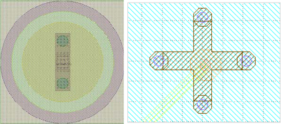
the rest, no connection would result. However, adding multiple (one or more) redundant TSVs for
each C4 connection, as shown in Figure 2, significantly increases the yield to the point where testing
may not be necessary.
If a customer deems interposer testing necessary, they add daisy chain structures at certain
strategic locations. Testing is usually done from the C4 side, where the pad diameter is 80 µm and
the pitch is 120 to 150 µm, allowing for simple cantilever probe cards for test. During interposer test,
if an open is detected in any of these test structures, the interposer die is marked as bad (unusable).
Figure 2: Redundant TSVs to C4 connection
ADVANCED PACKAGE TEST FLOW 6
Test Challenges with Advanced Packaging Technologies
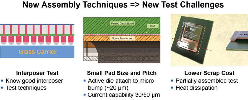
When the goal of an advanced package is to have high performance at a lower power budget,
the test requirements get pushed from “sub-speed testing” to “at speed testing.” Now the device has
to be tested for performance at the speed at which it is designed to operate and not a fraction of its
operational speed. This offers new challenges – such as making electrical contact, high-speed
performance of the probe card, high-current consumption of the device (at probe), bare-die handling
and heat dissipation (see Figure 3).
Figure 3: New Assembly Techniques provide New Test Challenges
To maintain signal integrity at high speeds, large sacrificial pads are replaced with small pads
that attach to the micro-bumps. The number of pins that make contact with the probe card can be in
the range of 20,000. With a 5-gm force per probe needle, the probe card core can experience over
100 Kg of force, making it susceptible to bending and reducing planarity. Furthermore, device
operating currents could well be in the 10’s of amperes range, limiting the choice of needle
technology. Running the device at speed, while checking for performance, creates large amounts of
heat. To prevent thermal runaway, the die is tested at subzero temperatures requiring special gaskets
to prevent condensation and water/ice buildup on the tester-prober interface.
ADVANCED PACKAGE TEST FLOW 7
When devices are built using the advanced packaging technologies with multiple
components, each with a yield Y
i
, the combined yield can be represented as:
Y
combined
= Y
substrate
* Y
interposer
* Y
die1
* Y
die2
* Y
die3
*….
In such cases, where multiple dies are added to a device, it becomes necessary to test the
partially-assembled device after each die is added to the build to reduce scrap costs. For economic
reasons, OEMs may opt to skip testing the partially assembled units, when components of very high
yield are added to the build.
Testing partially assembled devices at FT and SLT while operating at full speed brings new
challenges to test, such as handling partially assembled units with exposed die. The risks added by
testing at this stage are chipped edges, cracked die or cracked packages. To keep device temperatures
under control, active thermal control systems are connected to chiller units to maintain constant
device temperature. Additionally, partially assembled devices require electrical insulation to prevent
shorting of exposed pads and the chuck during test.
Adapting Existing Equipment for Advanced Package Test
When testing advanced packages, OSATs prefer to leverage existing assets rather than invest
in one-of-a-kind testers or material handlers (see Figure 4). For interposer testing, the incoming
requirement at test is to have the thinned 100 µm interposer wafers mounted on a 700 µm glass
carrier. This allows standard probers to handle the interposer wafer as a full thickness wafer.
Testing active dies with small pad sizes and pitch, requires probers with 1 µm accuracy and
the ability to apply up to 400 Kg of force. Thermal control of the die is achieved by adding the
optional chiller units to the prober that allow the chuck temperature to be lowered to -40°C.
Standard handlers are equipped with active thermal control (ATC) heads with each head
having its own heater / chiller unit. In more sophisticated implementations, the active thermal control