circuit of HS60.pdf - 第157页
5 - 25 0033638 6-010 101ND 4 854 boar d, axis r ear pane l HS-6 0 0033638 7-010 101ND 4 854 boar d, axis r ear pane l HS-6 0 A = Identificat ion label B = Inspection label Pinch off ke y pins. G32918-K0083-B 001-*-0017 2…
5 - 24
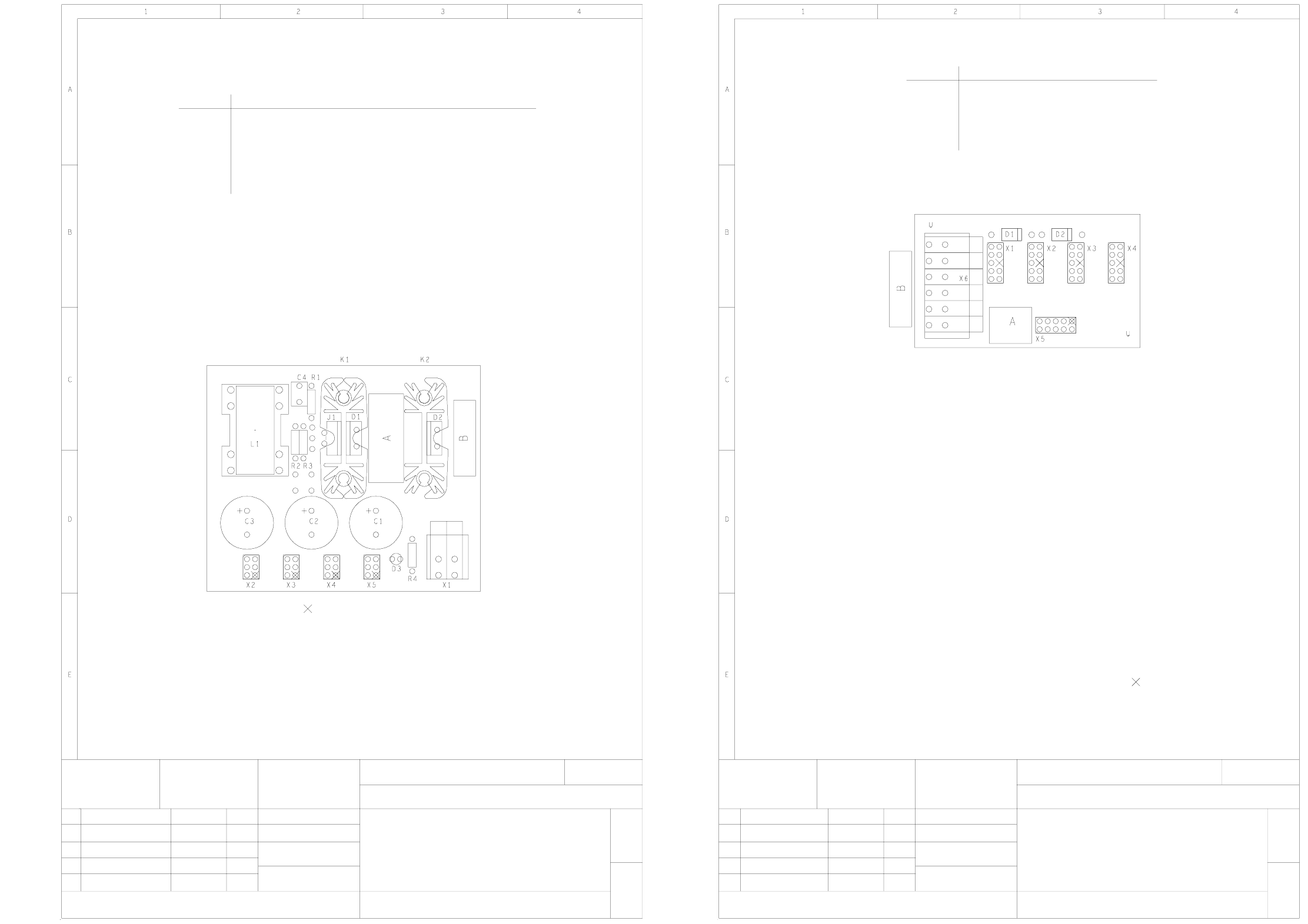
00336179-010101ND4 852, Stromversorgung SM motors
00336188-010101ND4 857 board, distributor f. illumination and flash HS-60
01 28.01.98 KL
ATD TD MCH 2
SIEMENS AG
23.01.98
Klose
Mounting diagram, component side
2-layer PC board
852 board
Power supply
G32918-K0053-B001-*-0017
00336179-010101ND4
1
1
SM motors
= pinch off key pin
A = ID label
B = inspection label
Insert an insulating foil between J1, D1, D2 and the heat sink.
Stat. Modified Date Name
Date
Name
Scale 1:1
Sheet
Sh.
Assembly
1, 3
2, 4
X5
X4
X3
X1
X2
Connector
To X10ca gantry distributor 3, + 15 V, step motors, gantry 3
To X10da gantry distributor 4, + 15 V, step motors, gantry 4
To X10ba gantry distributor 2, + 15 V, step motors, gantry 2
+ 30 V
To X10aa gantry distributor 1, + 15 V, step motors, gantry 1
GND
4
31
2
09.03.98
Klose
09.03.98 KL01
Stat. Modified Date Name
Date
Name
Scale 1:1
Sheet
Sh.
To X7th control unit 00334808, flash line
To X9ca, gantry distributor 3, 00335413
Assembly
To X9da, gantry distributor 4, 00335413
To X9ba, gantry distributor 2, 00335413
To X9aa, gantry distributor 1, 00335413
X5
X4
X1
X2
X3
Connector
+ 5 V VZ illumination
4 + 24 V illumination 2
6
5 + 24 V illumination 3
GND
2
3
1
+ 24 V PCB illumination
+ 24 V illumination 1
Connector X6
71
28
39
410
511
612
A = Identificaton label
B = Inspection label, lateral to X6
Pinch off key pin
G32918-K0085-B001-*-0017
2-layer printed circuit board
Mounting diagram, component side
857 board
Distributor, illumination
and flash HS60
00336188-010101ND4
1
1
ATD TD MCH 2
SIEMENS AG
5 - 25
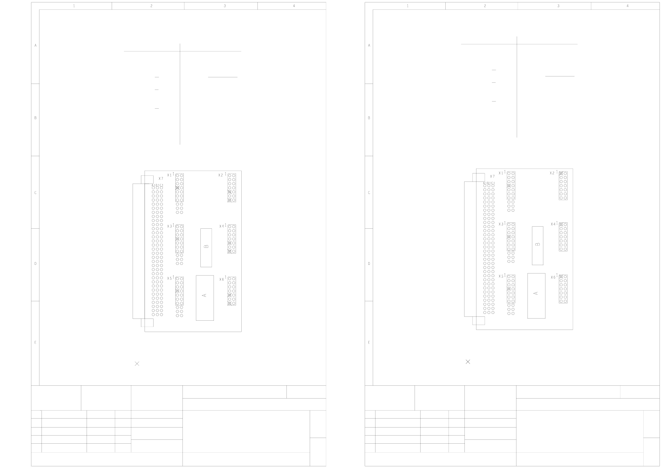
00336386-010101ND4 854 board, axis rear panel HS-60
00336387-010101ND4 854 board, axis rear panel HS-60
A = Identification label
B = Inspection label
Pinch off key pins.
G32918-K0083-B001-*-0017
2-layer printed circuit board
Mounting diagram, component side
854 board
Axis rear panel HS60
00336386-010101ND4
1
1
ATD TD MCH 2
SIEMENS AG
06.03.98
Klose
06.03.98 KL01
Stat. Modified Date Name
Date
Name
Scale 1:1
Sheet
Sh.
X1 / X3 / X5
1, 4
2
3
5
6
7
8
9
10
11
12
13
14
1, 8, 14
2
3
4
5
6
7
9
10
11
12
13
X2 / X4 / X6
Pin Pin
Track B
Key, Screen
Track N
Track N
Track B
Clamping
Reference point
Limit switch
Sensor stop
Opto coupler
Track A
Track A
Screen
Input 1
AGND
Key
ANA-2
Key
ANA-3
Input 2
ANA-1
Servo Ready
Servo Enable
Servo Enable
Screen
A = Identification label
B = Inspection label
Pinch off key pins
G32918-K0083-B001-*-0017
2-layer printed circuit board
Mounting diagram, component side
854 board
Axis rear panel HS60
00336387-010101ND4
ATD TD MCH 2
SIEMENS AG
06.03.98
Klose
06.03.98 KL01
02 06.04.98 KL
Stat. Modified Date Name
Date
Name
Scale 1:1
Sheet
1Sh.
1
Track B5
14
13
12
11
10 Opto coupler
Sensor stop
Limit switch
Reference point
Clamping
Track B
Track N
Track N
Key, Screen
8
9
7
6
Pin
1, 4
X1 / X3 / X5
Screen
Track A
Track A
2
3
Servo Enable3
13
12
11
10
9
7
6
4
AGND
ANA-2
Force
ANA-1
Input 2
ANA-3
Vnom
Servo Ready
Screen
Servo Enable
X2 / X4 / X6
2
8, 14
1
Pin
Key, screen
Input 15
5 - 26
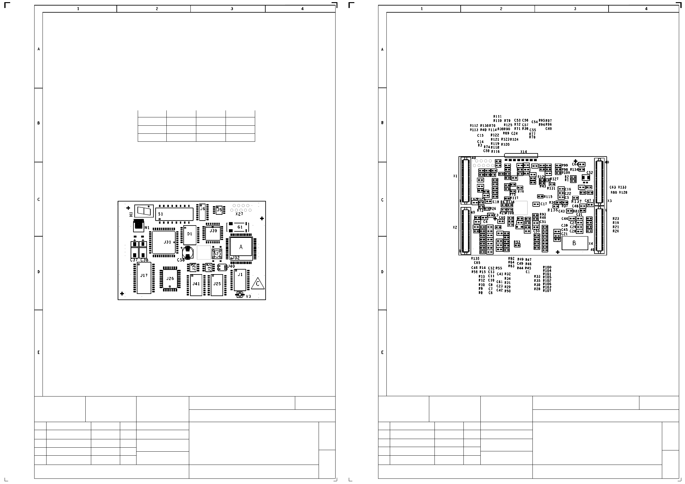
00344485-010101ND4 877 board, processor board 80C515C (Sh. 1 of 2)
00344485-010101ND4 877 board, processor board 80C515C (Sh. 2 of 2)
ESD label
Inspection label on solder side
Identification label on J32
- - - - - - -
- - - - - - -
- - - - - - -
01
03
02
07.12.98
KL
06.07.00
03.01.99
KL
KL
A
C
B
G32918-K0113-B001-*-0017
00344485-010101ND4
8-layer PCB
80C515C
Processor board
Mounting diagram, component side
ATD TD MCH 2
SIEMENS AG
Klose
07.12.98
PCB 877
1 +
Sheet
ZUST. MODIFIED DATE NAME
DATE
NAME
Scale 1 : 1
S1
1
2
3
4
5
6
7
8
ON
ON
ON
ON
OFF
OFF
OFF
OFF
ON
ON
OFF
ON
ON
ON
ON
OFF
ON
ON
OFF
OFF
Gantry 2Gantry 1 Gantry 3 Gantry 4
- - - - - - -
- - - - - - -
- - - - - - -
01
03
02
07.12.98
KL
06.07.00
03.01.99
KL
KL
G32918-K0113-B001-*-0017
00344485-010101ND4
8-layer PCB
80C515C
Processor board
Mounting diagram, component side
ATD TD MCH 2
SIEMENS AG
Klose
07.12.98
PCB 877
2 -
Sheet
ZUST. MODIFIED DATE NAME
DATE
NAME
Scale 1 : 1