OM-1683-001_w.pdf - 第78页
61 OM-1683 1 103-001 16.Specications Item Description 4. Applicable PCB Size X × Y Dual T ransfer Mode : 50 × 84 to 610 × 250 mm Single T ransfer Mode : 50 × 84 to 610 × 415 mm Note : Four Corners : R1 to R1.5 mm Thick…
60
OM-1683
1103-001
16.Specications
16.Specications
Item Description
1. Model GS-CU300
2. Applicable Model SIGMA-G5
3. PCB Flow
Direction
and Transfer
Reference
PCB Flow Direction :
From Left to Right
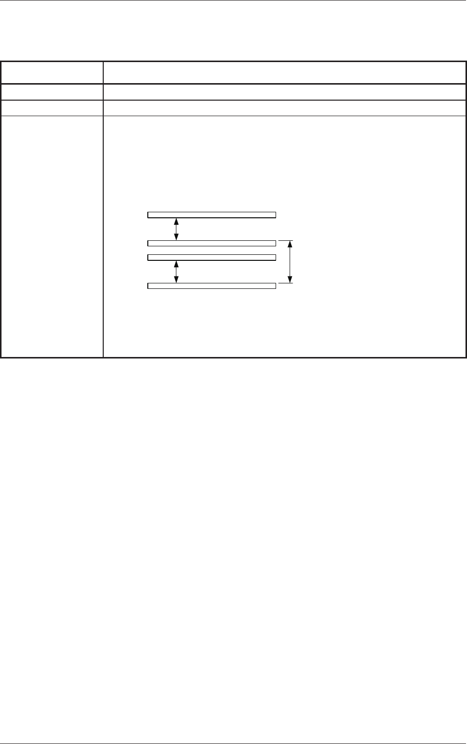
Transfer Reference : Lane A : Rear Right
Lane B : Front Right
Reference Chute : Lane A : Chute A
Lane B : Chute B'
Note
Rear Side of Machine
Front Side of Machine
Lane A
Lane B
Chute B’ (Fixed) : Reference
Chute B (Movable)
Chute A’ (Movable)
Chute A (Fixed) : Reference
250 mm or less
250 mm or less
Note : This unit does not comply with the transfer reference for the SMEMA
(size = 251 mm).
61
OM-1683
1103-001
16.Specications
Item Description
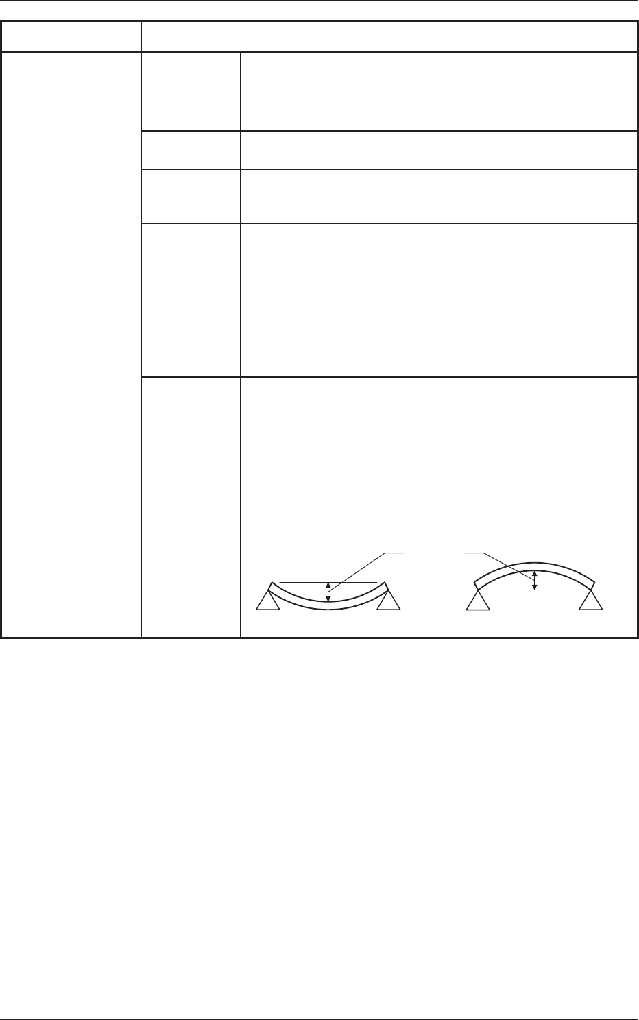
4. Applicable PCB Size
X × Y
Dual
Transfer Mode : 50 × 84 to 610 × 250 mm
Single Transfer Mode : 50 × 84 to 610 × 415 mm
Note :
Four Corners : R1 to R1.5 mm
Thickness 0.3 to 5.0 mm
Mass Max. 1.5 kg (50 <= X <= 260 mm)
Max. 2.
5 kg (260 < X <= 610 mm)
Material Glass Epoxy
Ceramic (Option)
Notes :
(a) In the case of ceramic, separate consideration is
required.
(b)
Depending on the PCB material, shape, warpage, mass
or surface condition (gloss), etc., it should be tested
whether or not the PCB can be transferred, or the
components can be placed normally, to conrm.
Warpage 0.2 mm or less per 50 mm (unit length)
Upper
: Max. 1.0 mm
Lower : Max. 1.0 mm
• 0.2 mm or less per 50 mm (unit length)
Example : The warpage must be 0.8 mm or less when the PCB size
is 200 mm.
• Max. 1.0 mm
Example : The warpage must be 1.0 mm or less when the PCB size
exceeds 250 mm.
Warpage
62
OM-1683
1103-001
16.Specications
Item Description
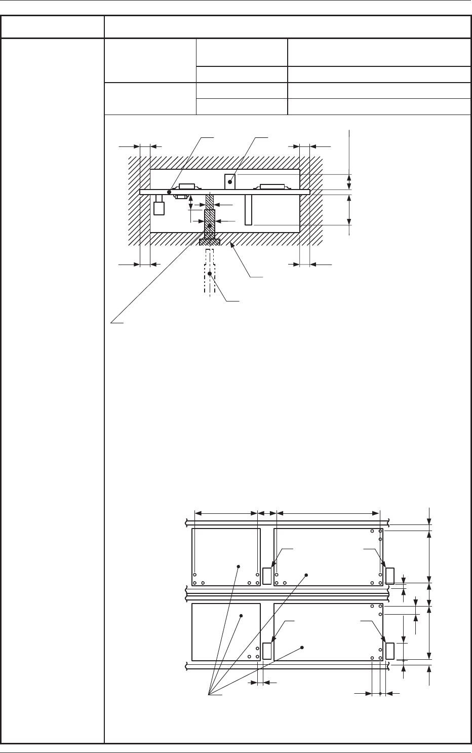
5. Conditions of PCB
before Placement
(Regulation
of Component
Height)
Height of
Previously Placed
Component
Upper surface 12.
7 mm / High-Speed Head
25.4 mm / Multi-Functional Head
Lower surface 30 mm
Dead Space
Upper surface 3.0 mm
Lower surface 3.0 mm
3.0
PCB
PCB Support Pin
(At this position when PCB is transferred.)
Previously placed Components
Placement Unallowed Range
Component
3.0
PCB Support Pin (Several Places)
φ5
φ2
4.0
3.0 3.0
When the High-Speed Head is used:
Max. 12.7
When the Multi-Functional Head is used:
Max. 25.4
Max. 30
(Front Side of Machine)
Unit : mm
Notes
: (a) The gure shows that the PCB is being supported.
(b) The PCB support pin is set onto the position where it does not touch any already
placed component.
(c) The dimensions are those for design reference.
Leave some room for the actual setting.
(d) The position of the PCB support pin can move by pitch of 10 mm.
(e) Even in the case that the same type of PCB is transferred in both the lane
A and
lane B, the PCB support pin setup positions are not the same.
(f) For the positional relationship between the conveyor, PCB stopper and backup
base, refer to the following gure.
230 10
55.5
50
250 300
9
230
10
30.5
10
5
Chute A
Lane A
Lane B
PCB Stopper
PCB Stopper
Backup Base
510
9
(Dual Transfer Mode : Flow from Left to Right)
Chute A'
Chute B
Chute B'
Unit : mm