N5194A矢量适配器数据表.pdf - 第3页
Page 3 Find us at www .keysight.com Spec ifications Frequency Range Specifie d r ange T unable rang e N5 194A with optio n 5 20 50 MHz to 20 GHz 1 0 MHz to 20 GHz N5 194A with optio n 540 50 MHz to 40 GHz 1 0 MHz to 44 G…

Page 2
Find us at www.keysight.com
Definitions and Conditions
Specification (spec): represents warranted performance of a calibrated instrument that has
been stored for a minimum of 2 hours within the operating temperature range of 0 to 50°C, unless
otherwise stated, and after a 1 hour warm–up period. The specifications include measurement
uncertainty. Data represented in this document are specifications unless otherwise noted.
Typical (typ): describes additional product performance information that is not covered by the
product warranty. It is performance beyond specifications that 80% of the units exhibit with a
95% confidence level at room temperature (approximately 25°C). Typical performance does not
include measurement uncertainty.
Nominal (nom): describes the expected mean or average performance, or an attribute whose
performance is by design, such as the 50 Ω connector. This data is not warranted and is
measured at room temperature (approximately 25°C).
Measured (meas): describes an attribute measured during the design phase for purposes
of communicating expected performance, such as amplitude drift vs. time. This data is not
warranted and is measured at room temperature (approximately 25°C).
All of the above apply when using the instrument in its default settings unless otherwise stated.
This data sheet provides a summary of the key performance parameters for UXG vector adapters.
All options referenced in this data sheet are described in the UXG vector adapter configuration
guide (5992–2332EN).
This is a combined data sheet for the N5194A UXG Vector Adapter and the N5192A
2
UXG
Vector Adapter, Modified version. Unless otherwise stated, all specifications, typical, nominal and
measured values described in this data sheet will be the same for the N5194A and N5192A and
apply:
– When the N5194A UXG vector adapter is used together with the N5193A UXG agile signal
generator with options EP1 enhanced phase noise, FR1 fine frequency resolution, SS2/SS4
switching speed, and CC1 LVDS I/O interface.
Note:
– The minimum options required for proper operation are SS2/SS4 switching speed and
the CC1 LVDS I/O interface.
– The N5194A UXG agile vector adapter 40 GHz model (option 540) only requires a 20 GHz
N5193A UXG agile signal generator to operate over its full 40 GHz frequency range.
– When the N5192A UXG vector adapter is used together with the N5191A UXG agile signal
generator with options FR1 fine frequency resolutions, SS3 switching speed and CC1 LVDS
I/O interface.
Note: The minimum options required for proper operation are SS3 switching speed and the
CC1 LVDS I/O interface.
The N5193A and N5191A provide the 6 GHz reference and LO signals necessary for operating the
N5194A and N5192A respectively.
1. Unless otherwise noted, this data sheet applies to units with serial numbers ending with xx6006xxxx or greater.
2. Because of the high-performance characteristics of the N5194A, a U.S. export license is required. The N5192A
is a modified version of the UXG agile vector adapter that provides high performance without requiring an
export license. Notable differences include maximum available frequency and switching speed.
Page 3
Find us at www.keysight.com
Specifications
Frequency
Range
Specified range Tunable range
N5194A with option 520 50 MHz to 20 GHz 10 MHz to 20 GHz
N5194A with option 540 50 MHz to 40 GHz 10 MHz to 44 GHz
N5192A with option 52E 50 MHz to 20 GHz 10 MHz to 20 GHz
CW frequency resolution
0.001 Hz
Phase offset
Adjustable in 0.1° increments
Accuracy
Accuracy is equivalent to the external frequency reference in use.
External 6 GHz reference input
Frequency 6 GHz
Input amplitude +5 to +15 dBm (nom)
Input impedance 50 Ω (nom)
Lower band 10 MHz to < 20.000000016 GHz
– Main lower band 50 MHz to < 20.000000016 GHz
– Extended lower band 10 MHz to < 50 MHz
Upper band 20.000000016 GHz to 44 GHz
– Main upper band 20.000000016 GHz to < 40 GHz
– Extended upper band 40 GHz to 44 GHz
1. RF CW switching speed using an external hardware trigger. Speeds apply for any combination of frequency, amplitude ≤ max specified power and phase
switching.
2. For indexed waveform mode and real-time pulse generation mode during PDW streaming operation, minimum pulse spacing is 240 ns. Certain frequency
transitions will result in longer spacing due to update rate (transition time) limitations as described on Page 3 and 4. Also refer to page 9 under “PDW
streaming” for more details.
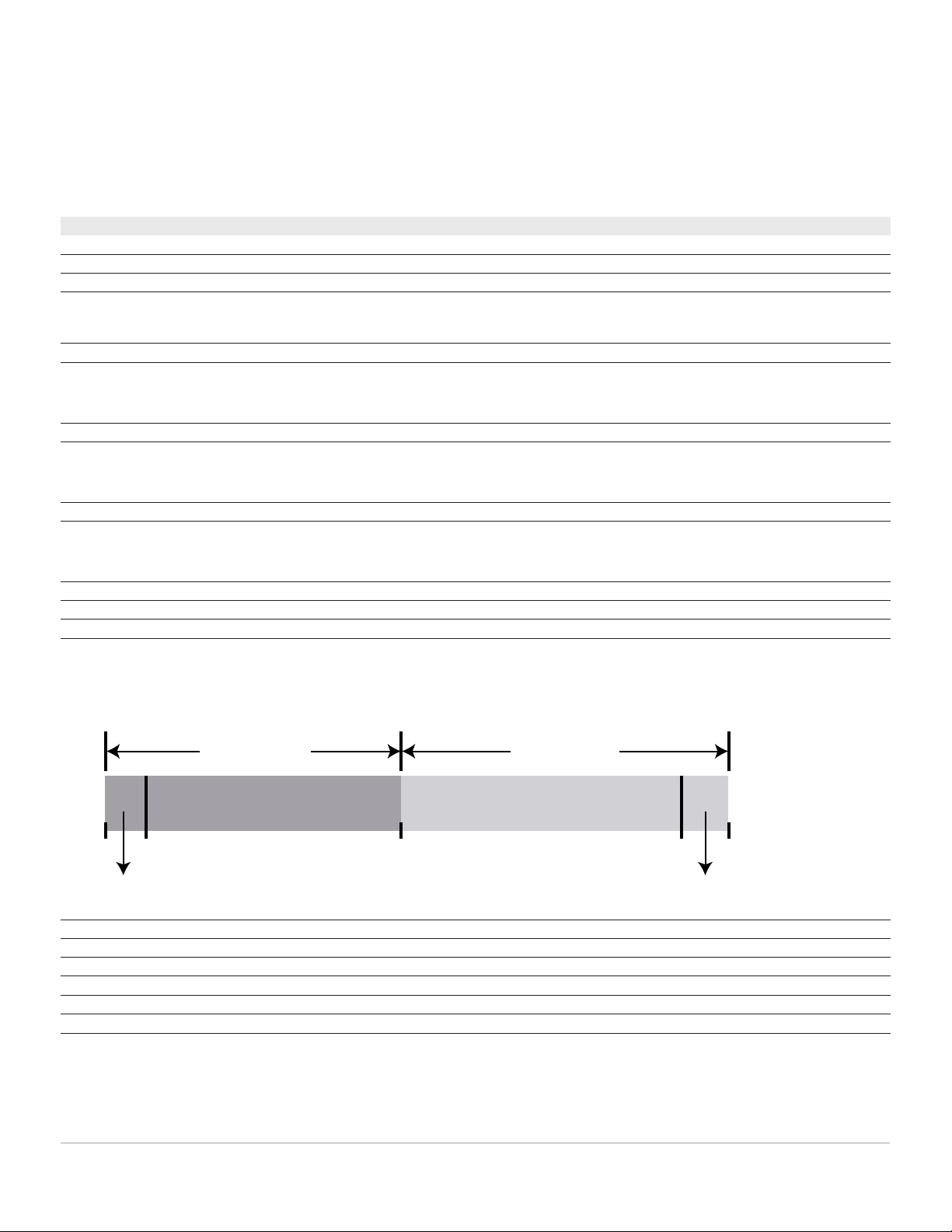
Switching speed for N5194A
1,2
Lower band Upper band
Main lower band Main upper band
40 GHz
20.000000016 GHz
44 GHz
10 MHz 50 MHz
Extended upper bandExtended lower band
Page 4
Find us at www.keysight.com
Latency (Nominal values)
Frequency
transitions
Transition details External LO mode,
narrowband,
nominal (µs)
External LO
mode, wideband,
nominal (µs)
Internal LO mode,
nominal (µs)
Internal LO mode,
Optimized
2
,
nominal (µs)
Within lower band Within main lower
band
3 2.5 3.5 3.5
Other transitions 3 2.5 3.5 —
Within upper band Within main upper
band
5 4.5 — —
Within upper
sub–bands
3
3 2.5 — —
Other transitions 5 4.5 — —
Between lower and
upper bands
Between main lower
and main upper
bands
5.5 5 — —
Other transitions 5.5 5 — —
RF phase settling criteria
Final frequency
10 MHz to < 2.85 GHz Measured to phase settled within 0.1 radians of final phase
2.85 GHz to < 8.64 GHz Measured to phase settled within 0.2 radians of final phase
8.64 GHz to < 17.3 GHz Measured to phase settled within 0.3 radians of final phase
≥ 17.3 GHz Measured to phase settled within 0.4 radians of final phase
Update rate (Transition time)
1
Frequency
transitions
Transition details External LO mode,
narrowband, spec
(typ)
External LO mode,
wideband, spec
(typ)
Internal LO mode,
spec (typ)
Internal LO mode,
Optimized
2
, spec
(typ)
Within lower band Within Main Lower
band
250 ns (190 ns) 220 ns (170 ns) 740 ns (470 ns) (210 ns)
Other transitions (250 ns) (220 ns) (250 ns) —
Within upper band Within Main Upper
Band
4.5 µs (2.5 µs) 4.5 µs (2.5 µs) — —
Within upper
sub–bands
3
(250 ns) (220 ns) — —
Other transitions (3.3 µs) (3.3 µs) — —
Between lower and
upper bands
Between Main
Lower and Main
Upper Bands
7 µs (4.3 µs) 7 µs (4.1 µs) — —
Other transitions (8 µs) (8 µs) — —
1. Update Rate is determined by the transition time as measured from the start of the RF transition (where the frequency, amplitude and phase are undefined)
to RF amplitude and phase settled. Latency is measured from the input trigger to RF amplitude and phase settled. For frequency transitions with typical
transition times of 2.5 us or longer, pre-pulse PDWs must be injected prior to the desired RF pulse to create clean pulses (except when using Simulation
View). Detailed descriptions of these pre-pulse PDWs can be found in the User’s Guide in the “Pre-Pulse PDW” section.
2. Optimized Mode applies when switching start frequency is not within any of the following 3 zones: (0 to 2.5 GHz) or (6.5 to 8 GHz) or (10 to 11.5 GHz), or stop
frequency is not within any of the following 2 zones: (13 to 14 GHz) or (18.5 to 20 GHz).
3. Upper sub bands include: 20.000000016 GHz to < 24.0 GHz
24.0 GHz to < 28.5 GHz
28.5 GHz to < 32 GHz
32 GHz to < 34 GHz
34 GHz to < 36 GHz
36 GHz to < 40.1 GHz
40.1 GHz to < 42 GHz
42 GHz to < 43.3 GHz
43.3 GHz to 44 GHz