00900002-01_UM_ASM-ProcessLens_EN.pdf - 第49页
3 Machine description 3.1 Overview of the modules Instruction Guide ASM ProcessLens 02/2017 49 1 Front board edge 2 Max. 2.5 mm 3 Conveyor rail 4 PCB transport direction 5 Max. 2.5 mm 6 Max. 3 mm 3.1.4.2 Maximum PCB warp…
3 Machine description
3.1 Overview of the modules
48 Instruction Guide ASM ProcessLens 02/2017
3.1.4 Definition of PCB warpage
This is the maximum allowable PCB warpage for the SPI to be able to measure accurately.
3.1.4.1 PCB warpage on the conveyor
PCB warpage across the direction of travel max. 1% of the PCB diagonal, but not exceeding
±5mm.
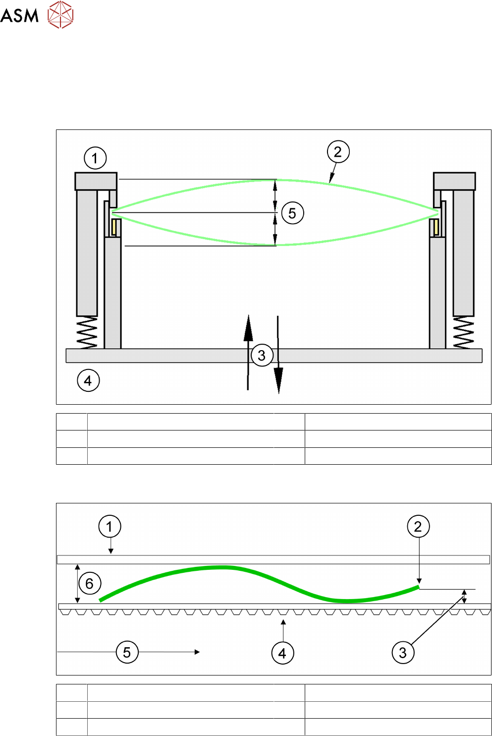
1 Fixed clamped edge 2 Printed circuit board
3 Movable clamping device 4 Conveyor rail
5 +/- 4.5 mm
PCB warpage in the direction of transport + PCB thickness < 5.5 mm. Bending up of board edge
max. 2.5 mm.
1 Fixed clamped edge 2 Front board edge
3 Max. 2.5 mm 4 Conveyor belt
5 PCB transport direction 6 5.5 mm
3 Machine description
3.1 Overview of the modules
Instruction Guide ASM ProcessLens 02/2017 49
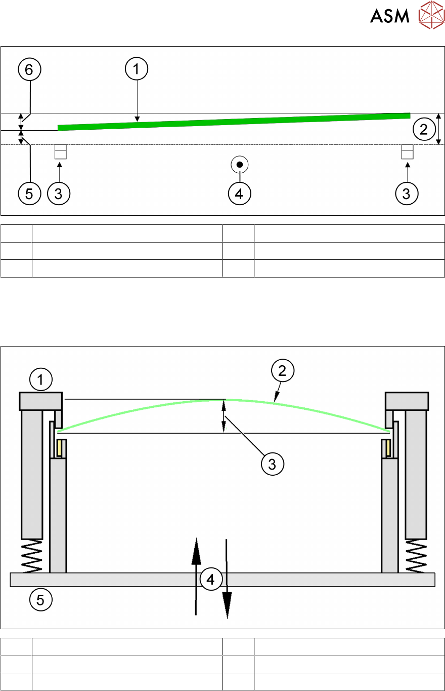
1 Front board edge 2 Max. 2.5 mm
3 Conveyor rail 4 PCB transport direction
5 Max. 2.5 mm 6 Max. 3 mm
3.1.4.2 Maximum PCB warpage allowed during processing of the board by ASM
ProcessLens
There is active PCB warpage measurement and tracking during the inspection so that images re-
main in sharp focus, ensuring best height measurement accuracy on the market.
1 Fixed clamped edge 2 Printed circuit board
3 ≤ 2 mm 4 Movable clamping device
5 Conveyor rail
PCB warpage down, max. 4.5 mm
3 Machine description
3.1 Overview of the modules
50 Instruction Guide ASM ProcessLens 02/2017
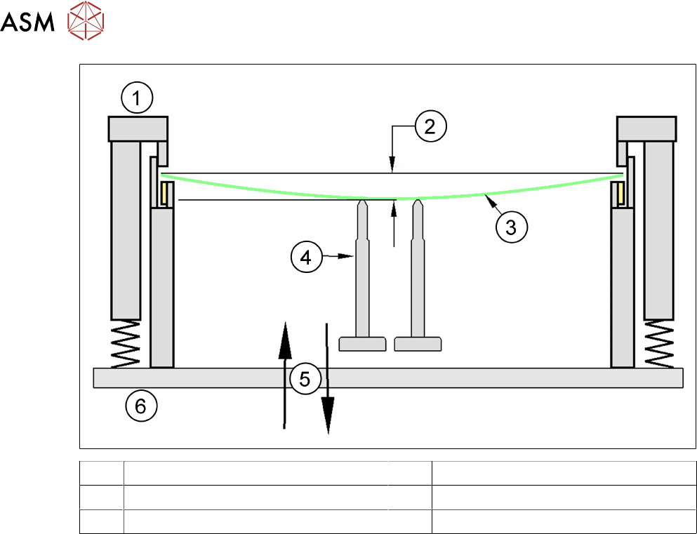
1 Fixed clamped edge 2 0.5 mm
3 Printed circuit board 4 Magnetic pin support
5 Movable clamping device 6 Conveyor rail
► Use magnetic pin supports to achieve this value.