ISM6636A&B_Rev1.10解密.pdf - 第16页
16 Innovision Semiconductor Preliminary Datas heet ISM6636 A/B Rev1.10 01/2023 user register V out_high_byte[0] an d user register V out_low_byte[7:0]. Over-current pro tection (OCP) and over- voltage prot ection (OVP) a…

15
Innovision Semiconductor
Preliminary Datasheet
ISM6636A/B
Rev1.10 01/2023
Functional Description
Overview
The ISM6636A/B is a family of small size,
low current, and high performance power
modules. It integrates output inductor and
capacitors for a complete system solution.
For ease of use, the module utilizes I2C
digital design to optimize power supply
parameters. The control topology allows no
external loop compensation while providing
fast transient response. Additional output
capacitors can be added for each rail
without any loop stability issue.
LDO Voltage
The ISM6636A/B uses an internal LDO
(Low Drop-Out) regulator to provide stable
bias voltage for the internal circuitries. The
nominal voltage of this LDO is 5V. This
device also supports external bias voltage
applications. If the external bias voltage is
used, the VIN pin and VCC pin should be
connected together to bypass the LDO. If
an single rail operation is desired, the VIN
pin must be connected to the PVIN pin.
When the supply voltage is above UVLO
threshold, the device is enabled regardless
of the configuration.
I2C Operation
The ISM6636A/B adopts the I2C digital
protocol to provide direct communication
between the device and the outside system.
The I2C communication begins as soon as
when VCC_UVLO start threshold is
exceeded, memory register is fully loaded,
the supply initialization is finished and the
address offset is fully read. The default
base address is 0x08. The offset 0-3 is then
determined by connecting ADDR pins to
AGND pins either directly or through a
resistor. The address detector reads the
resistance of the connection at startup and
uses it to set the offset. This offset is then
added to the base I2C address to set the
address with which the master device will
communicate.
To choose an offset from 0 to 3, follow the
instructions below.
• 0 – 0Ω (short ADDR to AGND) (0000
1000)
• +1 – 10kΩ (0000 1001)
• +2 – 20kΩ (0000 1010)
• +3 – >30.1kΩ (0000 1011)
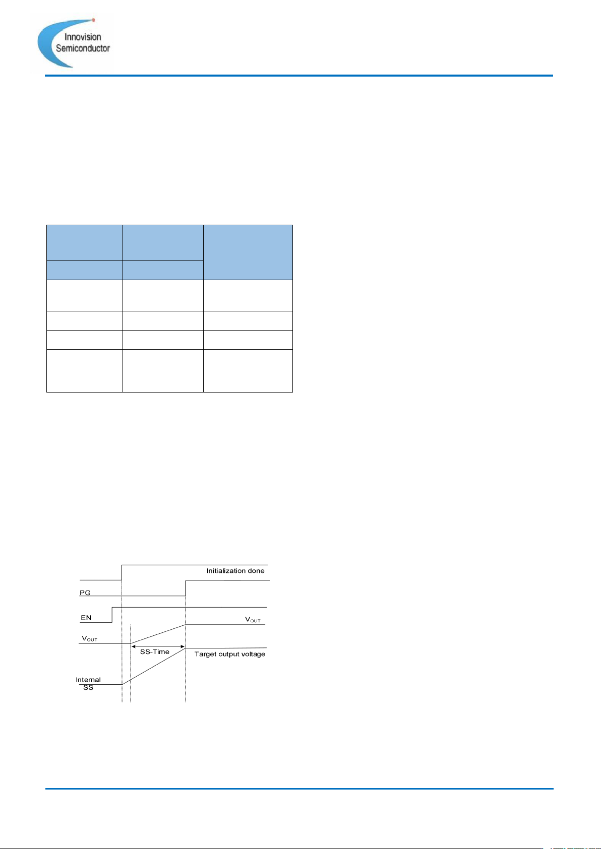
Soft-start Operation
The ISM6636A/B is designed to support a
smooth startup function with linearized
output voltage. This is accomplished by an
internal digital softstart circuit. When the
VCC exceeds the UVLO start threshold, the
loading of the contents of the non-volatile
memory into working register and
computing the address offset starts.
After the initialization is finished, Enable
(EN) pin is asserted (see Figure 1), the
internal reference voltage is soft-started to
the final target voltage level. The rate of
softstart is determined by the user register
bit SS_rate (see Table 1 below).
Register
Bits
Name/Description
0x14
[4:3]
SS_Rate:
00: 1mV/us, 01: 2mV/us
10: 0.5mV/us, 11: 4mV/us
Table 1 SS_Rate Register Description
During the initial softstart, the ISM6636A/B
uses minimum on time until the output
voltage rises. On time increases until VOUT
reaches the target value defined by the
16
Innovision Semiconductor
Preliminary Datasheet
ISM6636A/B
Rev1.10 01/2023
user register Vout_high_byte[0] and user
register Vout_low_byte[7:0].
Over-current protection (OCP) and over-
voltage protection (OVP) are both engaged
during soft start period to protect
ISM6636A/B from being damaged during
short circuit and over-voltage, respectively.
Table 2 SoftStopEnable and SoftDisable Register
Description
To achieve the best system accuracy, it is
recommended that the output voltage is
programmed by using the user registers
with appropriate codes. The output voltage
when programmed using the codes should
not be more than +/-20% of the preset
default voltage value.
Figure 1 Timing Diagram of Soft Start
Startup with Prebias
The ISM6636A/B supports smooth pre-bias
startup. When the output is pre-charged
with some voltage, both high side and low
side FETs are tri-stated. Once the internal
soft-start (SS) signal exceeds the output
voltage sensed at the VOS pin, the on-time
control is enabled which allows the turn-on
of the high side FET and followed by the
turn-on of the low side FET. The power
good circuit is not active until the first on
pulse is initiated.
Shutdown
The ISM6636A/B supports two ways of
shutting down.
1. Hard stop by Enable pin. When the
enable signal is forced low, both high side
and low side gate drivers are turned off
immediately. The internal softstart (SS)
signal is pulled down immediately as well.
The output voltage is discharged by the
load it is carrying.
2. Soft-stop by I2C register. When the user
register bit SoftStopEnable is set to 1 and
the user register bit SoftDisable is also set
to 1, the internal SS signal ramps down
following the same rate as it rises during
the initial softstart. Both gate drivers are
disabled only when the SS voltage reaches
0. The output voltage ramps down to 0 at
the rate set by the SS.
The ISM6636A/B does not support on the
fly change of SoftDisable bit when the
device is actively switching. For
applications that require soft-stop, this bit
must be set to 1. When EN pin is high, the
SoftStopEnable bit must be toggled to soft
start and/or soft stop the device. The
default shutdown mode for ISM6636A/B is
hard stop by EN pin.
SoftStop
Enable
SoftDisable
Description
0x14[2]
0x1C[3]
0
0
Use EN pin. Soft
Stop is disabled
0
1
Same as above
1
0
Same as above
1
1
Soft Stop is
active regardless
EN pin voltage
17
Innovision Semiconductor
Preliminary Datasheet
ISM6636A/B
Rev1.10 01/2023
Switching frequency
The switching frequency of the
ISM6636A/B is depend on the VOUT.For
the VOUT of 5V, the SW frequency is
normally 1.875MHz when the VOS is
connected to the VOUT.
Enable
The EN pin is used to enable or disable
ISM6636A/B. It has a precise threshold that
is monitored internally by the UVLO circuit.
If the EN pin is floating, the internal resistor
pulls it down to prevent the device from
inadvertently switching.
The EN pin can also be used to achieve
accurate input voltage UVLO. The input of
the EN pin is the PVIN voltage obtained by
a set of resistance dividers, REN1 and
REN2 (Figure 2). The user can program the
UVLO threshold voltage by selecting
different ratios. This will help to shut down
the device when the PVIN is below the
required voltage level.
The EN pin can be connected directly to the
PVIN without any external resistance
dividers. This is a useful feature when no
enable signals are available.
The EN pin can also be used to monitor
other power supplies for a particular power
sequencing arrangement (Figure 2).
Figure 2 Single Supply Configuration
Figure 3 External Bias Supply
Over-current protection (OCP)
The ISM6636A/B is designed with over
current protection function (OCP). The
current information is sensed through the
low side FET Rds_ON.The on-die OCP
provides accurate overcurrent protection
without the use of additional external sense
resistor. Since the current sense is done
on-die, the noise impact to the system is
minimized.
The OCP threshold is internally
temperature compensated, making it
almost constant at different ambient
temperatures.