ISM6636A&B_Rev1.10解密.pdf - 第34页
34 Innovision Semiconductor Preliminary Datas heet ISM6636 A/B Rev1.10 01/2023 PCB Layou t Guidelin es Efficient PCB la yout is crucial to the stable operation of the circuit. For best performance, refer to the f igure i…
33
Innovision Semiconductor
Preliminary Datasheet
ISM6636A/B
Rev1.10 01/2023
and compare it with the data in step 4 to verify the data. If the data is consistent, the
programming is successful. If it is inconsistent, perform steps 1~9 again.
Note: After performing step 8, the programming is successful. Users can choose to perform
step 9 for data verification to prevent system failures caused by external interference during
the programming process. The data loading of the OTP into the register will only be
performed after the VCC voltage reaches the start-up threshold voltage.
Command
User_OTP_ON
Format
unsigned binary
Bit
7
6
5
4
3
2
1
0
Access
R
R
R
R
R
R
R/W
R
Function
no use
User_OTP_ON
no use
Default
0
0
0
0
1
0
0
0
Table 29 Register = 0x1D
34
Innovision Semiconductor
Preliminary Datasheet
ISM6636A/B
Rev1.10 01/2023
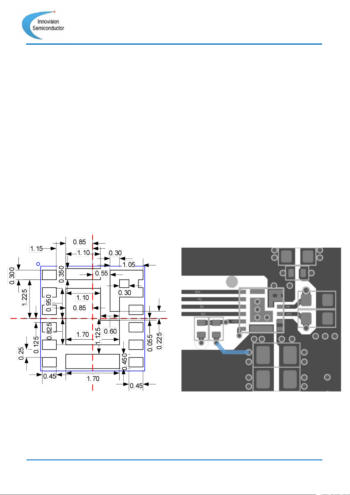
PCB Layout Guidelines
Efficient PCB layout is crucial to the stable operation of the circuit. For best performance,
refer to the figure in the PCB layout column and follow the PCB layout recommendations
below.
1. The input (output) MLCC capacitor shall be as close as possible to the VIN and
PGND(VOUT and PGND) pins and the main MLCC capacitor shall be placed on the
same wiring layer as ISM6636X. The copper plane of VIN,PGND,VOUT can be
maximized to minimize the parasitic impedance.
2. VCC and VIN capacitor should be placed as close to the ISM6636X as possible.
Connect PGND .
3. Place as many PGND holes as possible nearest to the PGND pin to minimize parasitic
impedance and thermal resistance.
4. AGND is connected to the PGND shortest path.
5. The VOS pin is far away from the interference source and connected to the remote
Vout capacitor.
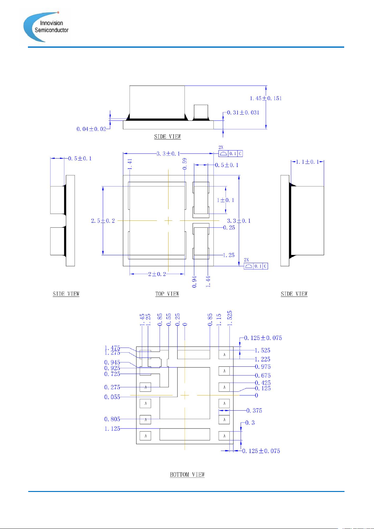
Recommended Land Pattern Recommended PCB layout