ISM6636A&B_Rev1.10解密.pdf - 第33页
33 Innovision Semiconductor Preliminary Datas heet ISM6636 A/B Rev1.10 01/2023 and compa re it with the data in ste p 4 to verify the d ata. If th e d ata is consistent, the programming is successf ul. If it is incon sis…
32
Innovision Semiconductor
Preliminary Datasheet
ISM6636A/B
Rev1.10 01/2023
Command
Status
Format
unsigned binary
Bit
7
6
5
4
3
2
1
0
Access
R
R
R
R
R
R
R
R
Function
Status_PG
Status_OVP
Status_OCP
Status_OTP
Status_Enable
no use
Default
0
0
0
0
1
0
0
0
Table 27 Register = 0x21
Register = 0x1D Unlock programming function (User_OTP_ON)
Register = 0x20 Burn times pointer (User_Pointer)
The ISM6636X will automatically load the default register values after power-on, and the
register value is stored in an OTP register. ISM6636X has 3 built-in OTP for upgrade use.
The factory defaults to use once, and the user can operate OTP to burn twice. The number
of times that can be programmed is recorded in register address 0x20 Bit [5:3]:
• Register address 0x20 [5:3] = 001 ; Indicates that OTP can be written twice, the
factory default.
• Register address 0x20 [5:3] = 011 ; Indicates that OTP can be written once more.
•
Register address 0x20 [5:3] = 111 ; Indicates that the OTP has no available counts.
Command
User_Pointer
Format
unsigned binary
Bit
7
6
5
4
3
2
1
0
Access
R
R
R
R
R
R
R
R
Function
no use
User_Pointer
no use
Default
0
0
0
0
1
0
0
0
Table 28 Register = 0x20
If the user needs to reconfigure and modify the default registers, the following steps can be
followed.
1. Set EN pin voltage low. Leave the module in an off state.
2. Make sure that the VIN or VCC voltage is normally powered.
3. To read the value of register 0x20 Bit [5:3], it is necessary to ensure that at least one
Bit = 0. If all are 1, it means that there are no available programming times, and the
operation is aborted.
4. Write the data to be modified into the register.
5. Write 0x02 to the register address 0x1D to unlock the programming function. After
power-on, the address 0x1D Bit[1] defaults to 0 to prevent user misoperation.
6. Write the command 0x15 to the register address 0x2B, the programming instruction
is executed, and the module will write the set value of the register into the new OTP mode.
7. Wait for 1 second. Do not power off VIN or VCC voltage while programming is in
progress.
8. After 1 second, the module programming is successful.
9. Restart the module (VIN and VCC are powered off to 0V and then powered on), at
this time the module will load the new OTP data into the register. Read the register data
33
Innovision Semiconductor
Preliminary Datasheet
ISM6636A/B
Rev1.10 01/2023
and compare it with the data in step 4 to verify the data. If the data is consistent, the
programming is successful. If it is inconsistent, perform steps 1~9 again.
Note: After performing step 8, the programming is successful. Users can choose to perform
step 9 for data verification to prevent system failures caused by external interference during
the programming process. The data loading of the OTP into the register will only be
performed after the VCC voltage reaches the start-up threshold voltage.
Command
User_OTP_ON
Format
unsigned binary
Bit
7
6
5
4
3
2
1
0
Access
R
R
R
R
R
R
R/W
R
Function
no use
User_OTP_ON
no use
Default
0
0
0
0
1
0
0
0
Table 29 Register = 0x1D
34
Innovision Semiconductor
Preliminary Datasheet
ISM6636A/B
Rev1.10 01/2023
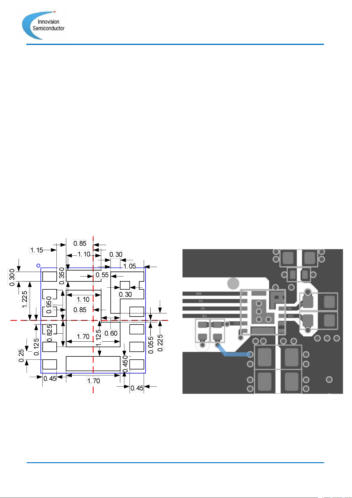
PCB Layout Guidelines
Efficient PCB layout is crucial to the stable operation of the circuit. For best performance,
refer to the figure in the PCB layout column and follow the PCB layout recommendations
below.
1. The input (output) MLCC capacitor shall be as close as possible to the VIN and
PGND(VOUT and PGND) pins and the main MLCC capacitor shall be placed on the
same wiring layer as ISM6636X. The copper plane of VIN,PGND,VOUT can be
maximized to minimize the parasitic impedance.
2. VCC and VIN capacitor should be placed as close to the ISM6636X as possible.
Connect PGND .
3. Place as many PGND holes as possible nearest to the PGND pin to minimize parasitic
impedance and thermal resistance.
4. AGND is connected to the PGND shortest path.
5. The VOS pin is far away from the interference source and connected to the remote
Vout capacitor.
Recommended Land Pattern Recommended PCB layout