ISM6636A&B_Rev1.10解密.pdf - 第19页
19 Innovision Semiconductor Preliminary Datas heet ISM6636 A/B Rev1.10 01/2023 has a built-in 20 ℃ hysteresis to prevent chattering. When th e OTP threshold is exceed ed, both high side an d low side FETs are turned off …
18
Innovision Semiconductor
Preliminary Datasheet
ISM6636A/B
Rev1.10 01/2023
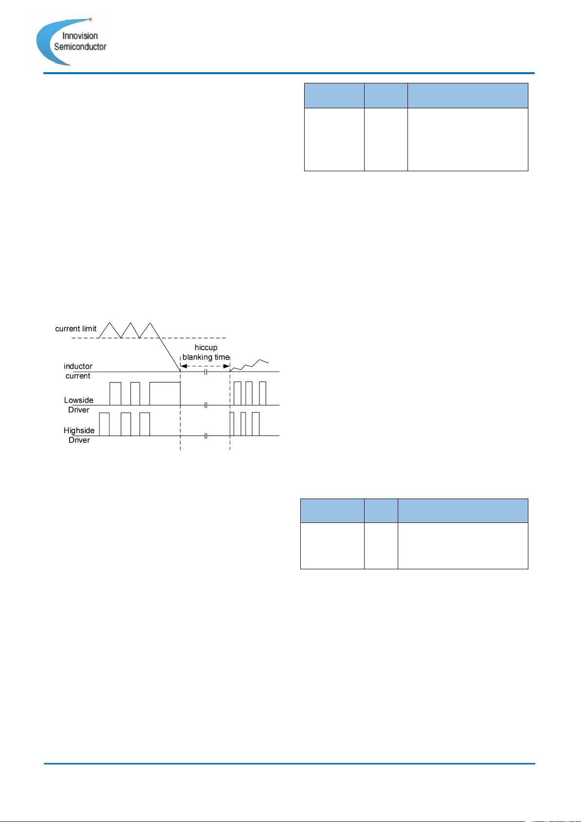
If the ISM6636A/B detects over-current
condition for 16 consecutive cycles and PG
signal is low, or the VOS falls below to 50%
of set value, the low side FET remains on
until the current falls to 0A, and then
ISM6636A/B enters hiccup mode (Figure 4).
Both the high side and low side FETs
remain off during the fault protection mode.
After the blanking time, ISM6636A/B will
attempt to restart. If the over-current fault is
still present, the above operation repeats
itself. The ISM6636A/B will remain in
hiccup mode until the over-current fault is
cleared.
Figure 4 OCP in Hiccup Mode
Over-voltage protection (OVP)
The ISM6636A/B is designed with over
voltage protection function (OVP). OVP is
provided by sensing the voltage at the VOS
pin. When the VOS exceeds the output
OVP threshold with greater than OVP delay
(usually 7μs), a fault condition will occur.
The OVP threshold is determined by the
user register bit OV_Threshold definition
(see Table 4 below).
Register
Bits
Name/Description
0x17
[1:0]
OV_SET:
00:105% of VOUT
01:110% of VOUT
10:115% of VOUT
11:120% of VOUT(default)
Table 4 OV_Threshold Register Description
When OVP happens, the high side FET is
turned off immediately and the PG pin is
pulled low. The low side FET is fully turned
on until the inductor current reaches zero.
Once zero crossing is reached, both high
side and low side FETs are tri-stated. When
the output voltage is discharged below the
reference voltage level, PWM starts
switching again. When the output voltage
falls below the 102.5% of reference level,
PG re-asserts.
If OV_Response register is set to 0, the
high side FET remains off until reset by
cycling VCC or EN signals. The voltage at
the VOS pin falling below the output OVP
threshold does not turn on the high side
FET, but it turns off the low side FET to
prevent the negative current from building
up.
Register
Bits
Name/Description
0x1A
[0]
OV_Response:
0:latch off
1:no latch off
Table 5 OV_Response Register Description
Over-temperature protection
(OTP)
When the on-die temperature falls within
the operating range, the device will
automatically restart. The OTP threshold
19
Innovision Semiconductor
Preliminary Datasheet
ISM6636A/B
Rev1.10 01/2023
has a built-in 20 ℃ hysteresis to prevent
chattering.
When the OTP threshold is exceeded, both
high side and low side FETs are turned off
and the internal SS circuit is pulled low. The
internal LDO regulator remains on during
an OTP fault.
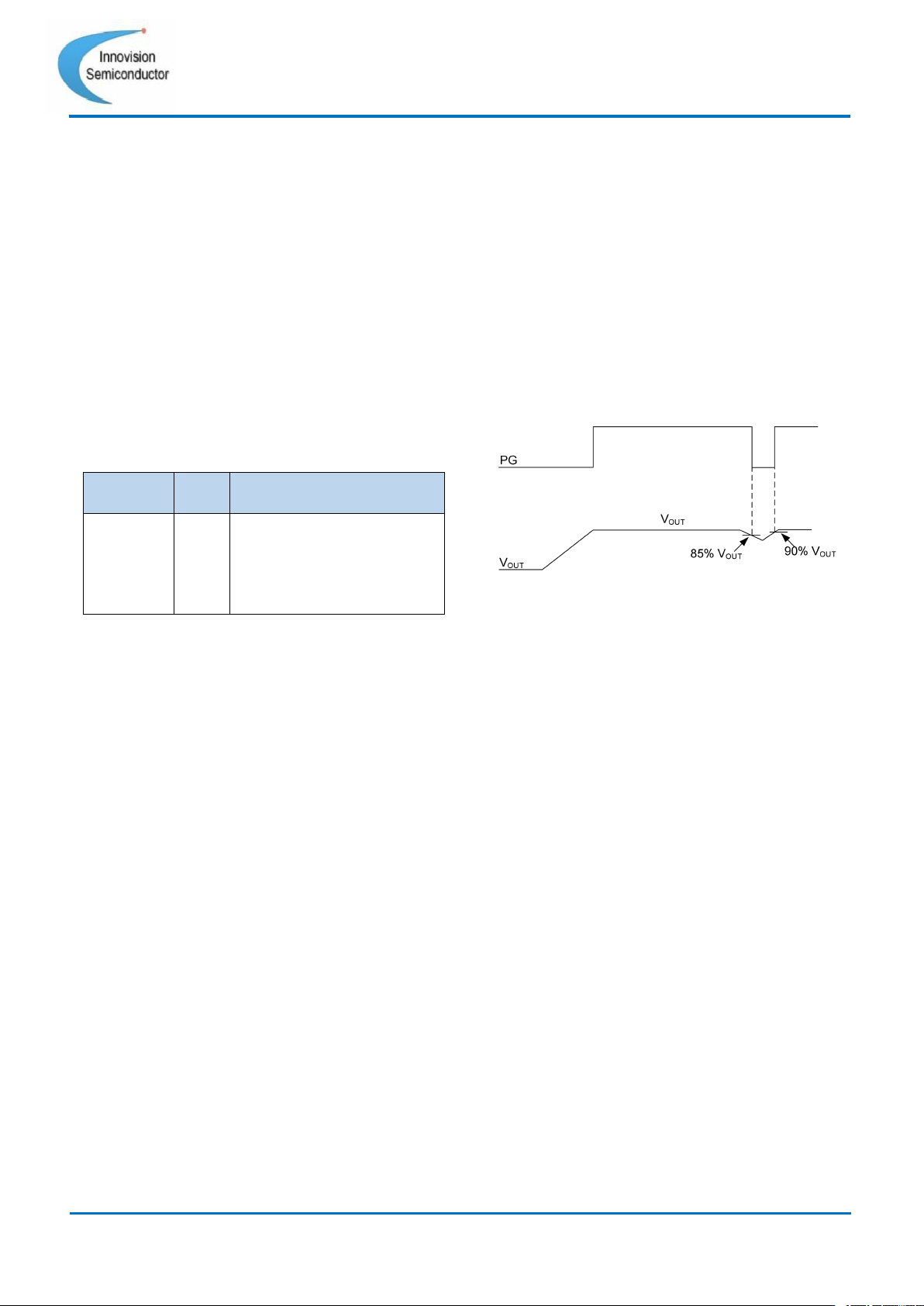
Power Good (PG)
The Power Good (PG) behavior is
determined by the user registers PG_
Threshold definition.
Register
Bits
Name/Description
0x18
[1:0]
PG_Threshold
0:80% of V
OUT
1:85% of V
OUT
2:90% of V
OUT
3:95% of V
OUT
The user register PG_Threshold defines
the upper PG threshold as the percentage
of Vout. For the lower PG threshold, a
hysteresis of 5% needs to be applied.
When VOS is higher than the upper
threshold, PG signal is asserted. When the
VOS drops below the lower threshold, the
PG signal will be de-asserted.
Figure 5 shows the PG behavior in this
case. In normal operation, when the output
voltage falls below the lower PG threshold,
the PG de-asserts; when the output voltage
rises above the upper PG threshold, the PG
asserts.
Figure 5 PG Signal
For pre-biased start-up, the PG signal will
not be activated until the first on time
control signal is generated.

20
Innovision Semiconductor
Preliminary Datasheet
ISM6636A/B
Rev1.10 01/2023
ISM6636X registers
Register Description
Reg
Name
Bits
Read
Write
Description
ISM6636A
Default
ISM6636B
Default
0x0A
Product_ID
[7:0]
R
Device identification.
0x36
0x36
0x0B
IC_Version
[7:0]
R
Silicon version.
0x01
0x01
0x0C
Pvin_Report
[7:0]
R
PVIN Range: 0->16V
1/16 V resolution.
\
\
0x0D
Vout_Report
[7:0]
R
Range: 0.8V --> 5.7V, 20mV
resolution.
\
\
0x0E
Iout_Report
[7:0]
R
Iout Range: 0A --> 8.2A
40mA Resolution.
\
\
0x0F
Temp_Report
[7:0]
R
Range: -40°C--180°C
1°C resolution.
\
\
0x11
Ramp_Amplitu
de
[3:0]
R/W
Adjust compensation ramp.
[3:0]=0110
[3:0]=0111
0x12
Vout_High_Bit
[0]
R/W
Set Vout voltage.
DAC Range 0.8V-->5.5V by
10mV step.
\
\
0x13
Vout_Low_Byte
[7:0]
R/W
\
\
0x14
Soft Start_Rate
[4:3]
R/W
[4:3]=00 : 1mV/µs;
[4:3]=01 : 2mV/µs;
[4:3]=10 : 0.5mV/µs;
[4:3]=11 : 4mV/µs;
[4:3]=00
[4:3]=00
Soft Stop
Enable
[2]
R/W
[2]=0: Disable; [2]=1: Enable;
[2]=0
[2]=0
FCCM and
DCM
[1]
R/W
If [1]=0 Select FCCM ;
If [1]=1 and EN<2.5V, Select
DCM.
If [1]=1 and EN>2.5V,Select
FCCM.
[1]=1
[1]=1
0x17
OV_Threshold
[1:0]
R/W
[1:0]=00 : 105%;
[1:0]=01 : 110%;
[1:0]=10 : 115%;
[1:0]=11 : 120%;
Default is 120%.
[1:0]=11
[1:0]=11
0x18
PG_Threshold
[1:0]
R/W
[1:0]=00 : 80%;
[1:0]=01 : 85%;
[1:0]=10 : 90%;
[1:0]=11 : 95%;
Default is 90%.
[1:0]=10
[1:0]=10
0x19
OT_Threshold
[1:0]
R/W
[1:0]=00 : 75°C;
[1:0]=01 : 85°C;
[1:0]=10 : 125° C;
[1:0]=11 : 145° C;
Default is 145° C.
[1:0]=11
[1:0]=11
0x1A
OV_Response
[0]
R/W
Behavior after triggering OV.
[0]=0 : Latch off;
[0]=1 : No-Latch off;
[0]=0
[0]=0