IPC-4552.pdf - 第20页
IPC-4552 Proposal June 2001 -0.15 -0.10 -0.05 0.00 0.05 0.10 0.15 0.20 0 0.38 0.75 1.13 1.5 1.88 2.25 2.63 3 3.38 3.75 4.13 4.5 4.88 5.25 5.63 6 6.38 6.75 7.13 7.5 7.88 8.25 8.63 9 9.38 9.75 time in seconds mN/mm 20 mins…

IPC-4552 Proposal June 2001
RESULTS:
As Received:
Due to the extensive XRF study on these panels, a time lag of approximately 90 days occurred between the time
they were plated and the time they were tested. For ease of publishing this document, only a small sample of the data
is presented here, the reader may request the more complete package from the author or from the IPC. The results
from the 90 day old samples showed very little in the way of performance differences between the two minute
plating dwell time samples (average of one (1) microinch gold) compared to the twenty minute plating dwell time
samples (average of four (4) microinches gold). See Fig 7 for Vendor E and Fig 8 for vendor D.
After Aging:
Since the introduction of the alternate finishes to tin/lead, the search for a suitable accelerated shelf life predictor has
been underway.
Steam aging: Steam aging the shell life predictor for Tin/Lead systems does not work for alternate finishes. ENIG
will produce non-solderable results from as little as one-hour exposure to steam; yet members of the committee have
anecdotal evidence of year plus shelf life being common and not an issue.
Temperature and Humidity (85°C/85% R.H): Members have tested at 85°C/85% R.H., 65°C/92% R.H., 160° C dry
bakes, all with varying degrees of impact on the solderability of the deposit. While not having a correlation for any
of these accelerating factors, the committee agreed upon 85°C/85% R.H to see if we could make a distinction in
soldering performance between the thinner (one microinch gold) versus the more typical (four microinch gold)
deposits.
The results from the wetting balance studies showed only a marginal improvement in performance for the thicker
deposits over the one microinch deposit. There was an increase in wetting time and the slope of the curve to
maximum wetting forces was affected more for the one microinch deposit. In both cases however the overall wetting
forces were reduced as a result of the exposure to 85°C/85% R.H. However it should be noted that the increase in
wetting times would not cause any issues in assembly of the product as they were shorter than the typical contact
times in a wave and did not have the benefits of either preheat or wave dynamics. Since the majority of ENIG coated
PWB’s are assembled using paste reflow techniques that have time above liquidus of 30 plus seconds as a
minimum, the increase in wetting times would have no significant effect on assembly.
Actual Aging:
At the time of writing this paper, the author came upon the original set of coupons from the test that were lying,
unprotected, in a tote bin in my office. These samples were now 240 plus days old since plating, (I knew there was a
reason I don’t clean my office). Samples from the two (2) minute plating dwell time (one microinch average gold
thickness) from Vendor’s D & E were again tested. The wetting times and performance remain excellent. It should
be noted that the effect of eight (8) plus months of unprotected storage was less than the effect of 18 hours of
85°C/85% R.H conditioning!
The author has for many years been conducting a solderability study in real time on all surface finishes using the
same test coupon and flux. As a point of interest I took the curves produced by the exposure to 18 hours of
85°C/85% R.H conditioning and attempted to match the curves with that from real time testing of
ENIG. The closest approximation would be 575 days of unprotected storage. The fact that a one microinch deposit
of gold can afford such a level of solderability protection is very impressive.
Page 17 of 10
Download From http://bbs.infoeach.com
Download From http://bbs.infoeach.com
IPC-4552 Proposal June 2001
-0.15
-0.10
-0.05
0.00
0.05
0.10
0.15
0.20
0
0.38
0.75
1.13
1.5
1.88
2.25
2.63
3
3.38
3.75
4.13
4.5
4.88
5.25
5.63
6
6.38
6.75
7.13
7.5
7.88
8.25
8.63
9
9.38
9.75
time in seconds
mN/mm
20 mins plating (4uins)
2 mins plating (1 uins)
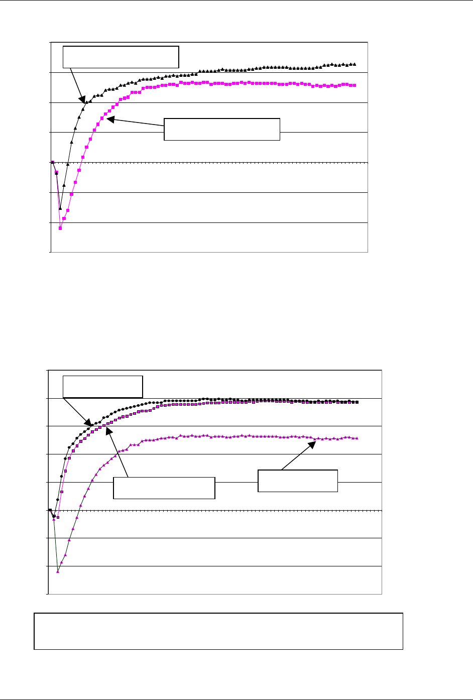
Fig 9: Wetting balance data for Vendor D post 18 hours 85/85 conditioning
-0.15
-0.1
-0.05
0
0.05
0.1
0.15
0.2
0.25
0
0.375
0.75
1.125
1.5
1.875
2.25
2.625
3
3.375
3.75
4.125
4.5
4.875
5.25
5.625
6
6.375
6.75
7.125
7.5
7.875
8.25
8.625
9
9.375
9.75
time
mN/mm
Fig 10: Comparison of one microinch gold deposit tested at 8 months shelf life
Vs as received & 85/85
90 DAYS OLD
8 MONTHS OLD
POST 85/85
Page 18 of 10
Download From http://bbs.infoeach.com
Download From http://bbs.infoeach.com
IPC-4552 Proposal June 2001
-0.15
-0.10
-0.05
0.00
0.05
0.10
0.15
0.20
0.25
0
0.375
0.75
1.125
1.5
1.875
2.25
2.625
3
3.375
3.75
4.125
4.5
4.875
5.25
5.625
6
6.375
6.75
7.125
7.5
7.875
8.25
8.625
9
9.375
9.75
tim e in seconds
mN/mm
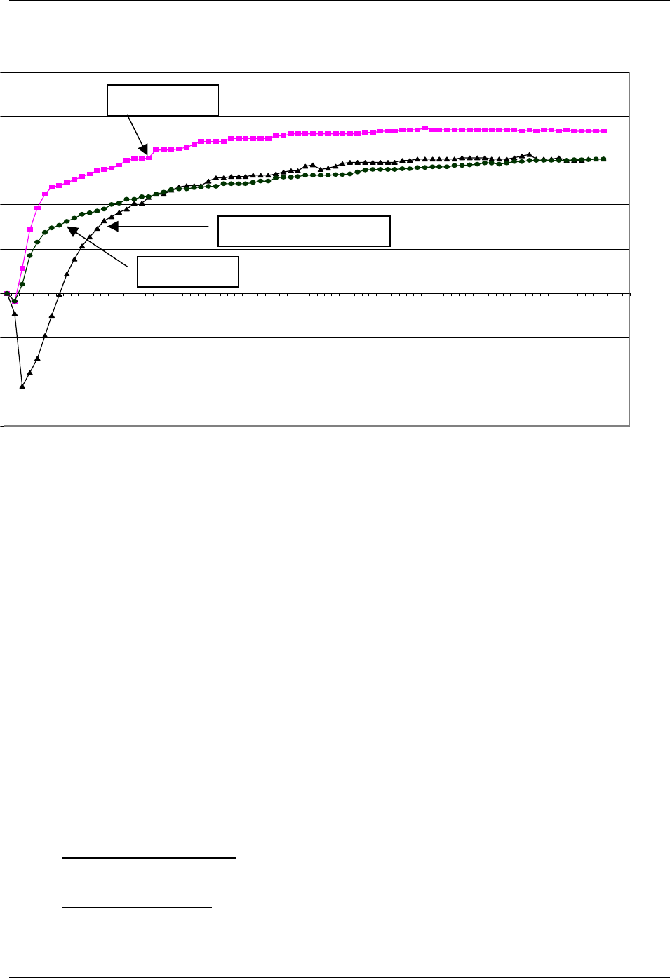
18 hrs 85C/85% R.H.
575 days old
90 days old
APPENDIX 5 Fig 11: Comparison of one microinch Gold deposit after various storage times /
conditions
With all the data from the above testing the task of determining the deposit ranges began to be a simpler if not still a
very controversial task. Based on the performance of the one microinch gold deposit, it was felt that by doubling this
thickness as the minimum value would provide the end user with a significant amount of shelf life, there being very
little in the way of solderability performance improvements for the thicker deposits. Controversy with regard to what
2 microinch minimum actually meant raised the following points:
1) Was it the minimum average?
2) Was it the absolute minimum?
3) Would you accept a data point at 1.99 microinches?
Following some heated discussions the group proposed the following - the minimum gold thickness deposit is 2
microinches at minus four standard deviations from the mean value.
Based on all the testing to date and the input on plating times from the five chemical suppliers, a typical gold deposit
thickness range will be in the 3 to 5 microinches. A number of committee members looked to have an upper
specification for the gold thickness. We believe that it is not necessary as the reaction is self-limiting and based on
the XRF data, some of the gold systems may never be able to achieve an upper specification number. What is most
important is not an upper number but rather the performance of the deposit, which is governed by the minimum
thickness of the gold. This maybe a good point to mention that Gold embrittlement is not an issue with ENIG over
the ranges of deposit thickness measured in the XRF study.
Based on these studies and industry consensus, the thickness specification was set at:
5.1.1 Electroless Nickel Thickness:
The electroless nickel thickness shall be 3 to 6 microns (120 to 240 µin).
5.1.2
Immersion Gold Thickness:
The minimum immersion gold thickness shall be 0.05 microns (2 µin) at four sigma below the mean; the typical
range is 3 to 5 µin. Setup and measurement methodologies are crucial for accuracy (see appendix for recommended
Page 19 of 10
Download From http://bbs.infoeach.com
Download From http://bbs.infoeach.com