IPC-4552.pdf - 第21页
IPC-4552 Proposal June 2001 -0 . 1 5 -0 . 1 0 -0 . 0 5 0.00 0.05 0.10 0.15 0.20 0.25 0 0.375 0.75 1.125 1.5 1.875 2.25 2.625 3 3.375 3.75 4.125 4.5 4.875 5.25 5.625 6 6.375 6.75 7.125 7.5 7.875 8.25 8.625 9 9.375 9.75 ti…
IPC-4552 Proposal June 2001
-0.15
-0.10
-0.05
0.00
0.05
0.10
0.15
0.20
0
0.38
0.75
1.13
1.5
1.88
2.25
2.63
3
3.38
3.75
4.13
4.5
4.88
5.25
5.63
6
6.38
6.75
7.13
7.5
7.88
8.25
8.63
9
9.38
9.75
time in seconds
mN/mm
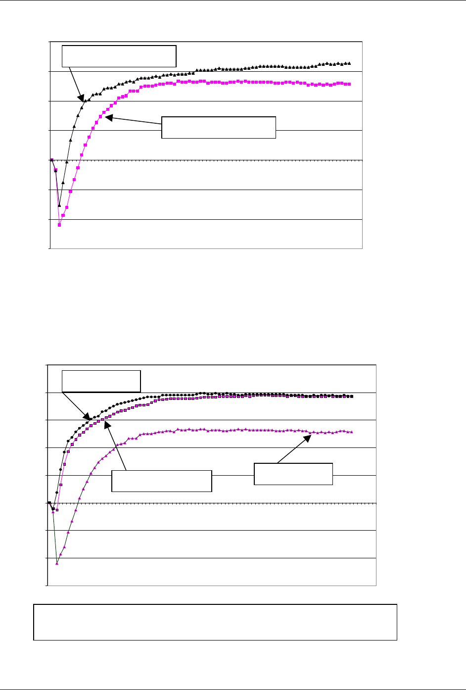
20 mins plating (4uins)
2 mins plating (1 uins)
Fig 9: Wetting balance data for Vendor D post 18 hours 85/85 conditioning
-0.15
-0.1
-0.05
0
0.05
0.1
0.15
0.2
0.25
0
0.375
0.75
1.125
1.5
1.875
2.25
2.625
3
3.375
3.75
4.125
4.5
4.875
5.25
5.625
6
6.375
6.75
7.125
7.5
7.875
8.25
8.625
9
9.375
9.75
time
mN/mm
Fig 10: Comparison of one microinch gold deposit tested at 8 months shelf life
Vs as received & 85/85
90 DAYS OLD
8 MONTHS OLD
POST 85/85
Page 18 of 10
Download From http://bbs.infoeach.com
Download From http://bbs.infoeach.com
IPC-4552 Proposal June 2001
-0.15
-0.10
-0.05
0.00
0.05
0.10
0.15
0.20
0.25
0
0.375
0.75
1.125
1.5
1.875
2.25
2.625
3
3.375
3.75
4.125
4.5
4.875
5.25
5.625
6
6.375
6.75
7.125
7.5
7.875
8.25
8.625
9
9.375
9.75
tim e in seconds
mN/mm
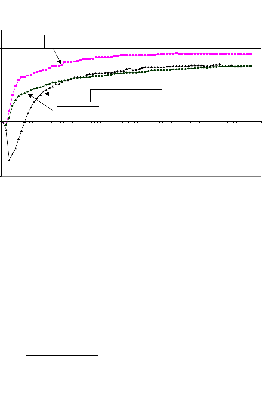
18 hrs 85C/85% R.H.
575 days old
90 days old
APPENDIX 5 Fig 11: Comparison of one microinch Gold deposit after various storage times /
conditions
With all the data from the above testing the task of determining the deposit ranges began to be a simpler if not still a
very controversial task. Based on the performance of the one microinch gold deposit, it was felt that by doubling this
thickness as the minimum value would provide the end user with a significant amount of shelf life, there being very
little in the way of solderability performance improvements for the thicker deposits. Controversy with regard to what
2 microinch minimum actually meant raised the following points:
1) Was it the minimum average?
2) Was it the absolute minimum?
3) Would you accept a data point at 1.99 microinches?
Following some heated discussions the group proposed the following - the minimum gold thickness deposit is 2
microinches at minus four standard deviations from the mean value.
Based on all the testing to date and the input on plating times from the five chemical suppliers, a typical gold deposit
thickness range will be in the 3 to 5 microinches. A number of committee members looked to have an upper
specification for the gold thickness. We believe that it is not necessary as the reaction is self-limiting and based on
the XRF data, some of the gold systems may never be able to achieve an upper specification number. What is most
important is not an upper number but rather the performance of the deposit, which is governed by the minimum
thickness of the gold. This maybe a good point to mention that Gold embrittlement is not an issue with ENIG over
the ranges of deposit thickness measured in the XRF study.
Based on these studies and industry consensus, the thickness specification was set at:
5.1.1 Electroless Nickel Thickness:
The electroless nickel thickness shall be 3 to 6 microns (120 to 240 µin).
5.1.2
Immersion Gold Thickness:
The minimum immersion gold thickness shall be 0.05 microns (2 µin) at four sigma below the mean; the typical
range is 3 to 5 µin. Setup and measurement methodologies are crucial for accuracy (see appendix for recommended
Page 19 of 10
Download From http://bbs.infoeach.com
Download From http://bbs.infoeach.com

IPC-4552 Proposal June 2001
measurement techniques).
One of the byproducts of such an extensive series of tests was the identification of the variability that exists between
ENIG suppliers and that while the deposit thickness values maybe different the performance from a base
solderability standpoint is the same. It is clear that, all involved in ENIG – supplier, board house and OEM – need
to quantify their individual processes and have the necessary data to demonstrate that the process is known and
understood from a statistical / chemical and solderability viewpoint.
Contact Resistance Testing:
One of the functions that ENIG provides as a surface finish is that of a contact resistance surface that typically
interfaces with a “soft touch” membrane keypad. The membrane is usually carbon impregnated but other metal
dome switches are also used for this type of application, (the group is still requesting performance data on this type
of switch). While the group had a lot of anecdotal evidence of its use, cell phones, keypads etc, nobody had data for
this type of switch that was not company specific and therefore not shareable with the IPC community. In an attempt
to obtain shareable data, the committee decided to test some different patterns commonly in use in the industry.
After much searching we came upon S/G Industries, a supplier of membrane overlays to the automotive industry
among others. With their help, three different designs were fabricated:
1) Interlocking Square contacts
2) Interlocking Round contacts
3) Half Moon contacts
Note: At the time of writing this paper, test data from only the Interlocking square pattern is available.
To increase the data set it was decided to have two of the ENIG chemical suppliers plate these patterns. The testing
would be run until failure or until the resistance change would be considered non-useable for the switch application.
From the data from the first pattern testing at the time of writing, it would appear that we will stop test at 2 million
cycles with no negative, i.e. increase in resistance, being evident. The committee feels that 2 million cycles is more
than adequate to prove the use of ENIG as a suitable surface for this type of application.
The test protocol was as follows:
1) Each PWB/keypad assembly consists of five (5) pads.
2) Each pad represents a different carbon contact and trace size ranging from 2.0mm to 4.0 mm.
3) A total of six assembly sets will be tested
4) There are two ENIG suppliers, Vendor’s C&E
5) Initial testing consists of applying a 1000 gram load to the entire keypad (1000 grams / 5 switches per
keypad = 200 grams per switch).
6) Initial resistance measurements are taken from each switch location with this force applied without
passing current through the switch (mechanical durability test only)
7) The PCB/keypad assembly is then actuated in 50,000 cycle intervals with resistance measurements
taken at each interval. The forces applied during resistance measurements are identical to those used
during the initial resistance measurements (200 grams per switch).
8) Reference of positions measured: Position 1: 2.0 mm carbon contact, Position 2: 2.5 mm carbon
contact, Position 3: 3.0 mm carbon contact, Position 4: 3.5 mm carbon contact, Position 5: 4.0 mm
carbon contact.
The results from 1.85 million cycles for the interlocking square pattern are detailed below.
As can be seen from this summary data set the general trend in the resistance data is down, the direction of choice.
In discussions with S/G Industries regarding these phenomena, they explained that the carbon particles that are
impregnated into the pill tend to be compacted as the switch is compressed over time. This therefore reduces the
contact resistance, which is clearly demonstrated in the above graphs. A visual
Page 20 of 10
Download From http://bbs.infoeach.com
Download From http://bbs.infoeach.com