IPC-4552.pdf - 第6页
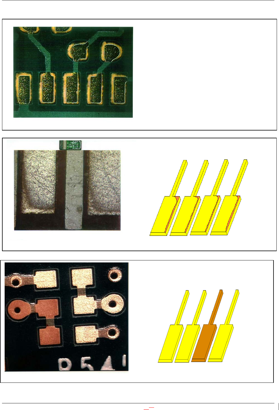
IPC-4552 Proposal June 2001 Fi g ure 3-2 Extraneous Platin g or Nickel Foot Figure 3-3 Edge Pull Back Figure 3-4Skip Plating Page 4 of 2525 Download From http://bbs.infoeach.com Download From http://bbs.infoeach.com
IPC-4552 Proposal June 2001
3 REQUIREMENTS
Table 3-1 Requirements of Electroless Nickel Immersion Gold Plating
Tests Test
Method
Requirement
Paragraph
Class 1 Class 2 Class 3
General
Visual Visual 3.1 Uniform plating and complete coverage of surface to
be plated
Electroless Nickel
Thickness
APPENDIX 4
3.2.1
3 to 6 µm
[118.1 to 236.2 µin]
Immersion Gold
Thickness
APPENDIX 4 0
0.05 µm minimum
[1.97 µin minimum]
Porosity N/A 3.3 N/A
Physical
Adhesion/Tape Test
IPC-TM-650
TM 2.4.1
3.4 No evidence of plating removed
Solderability
J-STD-003 3.5 Meet solderability requirements of Category 3
durability with 6 months shelf life.
Chemical
Phosphorous/Boron
Content
ASTM B733-
97 & ASTM
B607-91
(1998)
1.2.1 (Reference Only; Supplier Dependent – No Testing
Required)
Chemical Resistance N/A 3.7 N/A
Electrical
High Frequency
Signal Loss
(1)
3.8 TBD TBD TBD
Contact Resistance
(1)
1.4.2 TBD
Environmental
Cleanliness
IPC-TM-650
TM 2.3.25
3.6
Max. 1.56 µg/cm
2
(1)
An appropriate IPC-TM-650 test method used to generate data for this electrical property is not available at the
time of this writing.
3.1
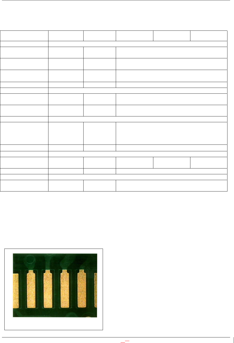
Visual
ENIG surfaces shall be inspected in accordance with the visual examination sections of the IPC-6011 series, and
specifically IPC-6012 which specifies a nominal magnification of 1.75X (approx. 3 diopters). The coverage shall be
complete and the finish shall be uniform on the surface to be plated (Figure 3-1). There shall be no extraneous
plating or nickel foot (Figure 3-2), edge pull back (Figure 3-3) or skip plating (Figure 3-4) on the plated surface for
all classes of product.
Page 3 of 2525
Figure 3-1 Uniform Plating
Download From http://bbs.infoeach.com
Download From http://bbs.infoeach.com

IPC-4552 Proposal June 2001
3.2
3.2.1
3.2.2
3.3
3.4
3.5
3.6
3.7
3.8
Finish Thickness
Thickness of the nickel and gold layers shall be measured and verified following the ENIG plating step in the PWB
fabrication process. The use of X-ray fluorescence methodology for thickness determination shall be in accordance
with APPENDIX 4 of this document and shall employ X-ray fluorescence (XRF) instrumentation equipped with
software and hardware specific for ENIG measurement. The XRF test method is per ISO-4527, Auto-Catalytic
Nickel-Phosphorous Coatings; Specifications and Test Methods.
Electroless Nickel Thickness
The electroless nickel thickness shall be 3 to 6 µm [118.1 to 236.2 µin].
Immersion Gold Thickness
The minimum immersion gold thickness shall be 0.05 µm [1.97 µin] at four sigma (standard deviation) below the
mean; the typical range is 0.075 to 0.125 µm [2.955 to 4.925 µin]. Higher gold thickness would normally require
extended solution dwell time and /or increased solution temperature. This can increase the risk of compromising the
integrity of the nickel undercoat due to excessive corrosion. Setup and measurement methodologies are crucial for
accuracy (see APPENDIX 4 for recommended measurement techniques).
Porosity
The ENIG immersion gold layer is not totally impervious and it will not pass the requirements of a ‘classic’ porosity
test (Nitric acid per ASTM B 735).
Adhesion
The purpose of adhesion testing for ENIG finished boards is two fold. The first is for testing the plating adhesion of
the immersion gold to the nickel as well as the nickel to the underlying metals. The second is for testing the
adhesion of the solder mask to both traces and laminate. In both cases testing should be conducted on regions of
high density on the board such as BGA sites, dams between fine pitch leaded devices or over areas of high trace
density. The tape testing will be in accordance with IPC-TM-650, test method 2.4.1 using a strip of pressure
sensitive tape. There shall be no evidence of any portion of the surface finish or the soldermask being removed, as
shown by particles of plating/pattern or soldermask adhering to the tape.
If overhanging metal (slivers) or soldermask undercut breaks off and adheres to the tape, it is evidence of overhang
or slivers, but not of adhesion failures.
Because of the requirement to test in high density areas, the potential to leave tape residue that could interfere with
soldering exists, especially if the wrong type of tape is used. Verification of zero impact to solderability must be
demonstrated for the areas tested.
Solderability
This thickness specification contained herein shall meet the coating durability requirements of Category 3 in J-STD-
003, i.e. greater than 6 months shelf life. Note: the use of steam aging (conditioning) is not an applicable accelerated
aging (stress) test method for ENIG.
Cleanliness
The ENIG finish typically will result in a surface that is cleaner than most other surface finishes. The process shall
be installed and maintained using IPC-TM-650, Test Method 2.3.25 Detection and Measurement of Ionizable
Surface Contaminants by Resistivity of Solvent Extract, and shall meet the values given in IPC-6011 series of 1.56
µg/cm
2
NaCl equivalent. Failure to meet this cleanliness specification should trigger immediate corrective action.
Chemical Resistance
Chemical resistance testing of the ENIG finish is not applicable.
High Frequency Signal Loss
Higher frequency (>1 GHz) applications may experience signal loss due to increase electrical resistance (skin
effect). Due to electrical differences such as this, special considerations should incorporated for any edge-coupled
Page 5 of 2525
Download From http://bbs.infoeach.com
Download From http://bbs.infoeach.com