IPC-4552.pdf - 第8页
IPC-4552 Proposal June 2001 structures on the outer layers. This impact will b e more prevalent when ENIG is ap plied over all copper f eatures, such as application of ENIG before so lder mask. This impact is m inimized …

IPC-4552 Proposal June 2001
3.2
3.2.1
3.2.2
3.3
3.4
3.5
3.6
3.7
3.8
Finish Thickness
Thickness of the nickel and gold layers shall be measured and verified following the ENIG plating step in the PWB
fabrication process. The use of X-ray fluorescence methodology for thickness determination shall be in accordance
with APPENDIX 4 of this document and shall employ X-ray fluorescence (XRF) instrumentation equipped with
software and hardware specific for ENIG measurement. The XRF test method is per ISO-4527, Auto-Catalytic
Nickel-Phosphorous Coatings; Specifications and Test Methods.
Electroless Nickel Thickness
The electroless nickel thickness shall be 3 to 6 µm [118.1 to 236.2 µin].
Immersion Gold Thickness
The minimum immersion gold thickness shall be 0.05 µm [1.97 µin] at four sigma (standard deviation) below the
mean; the typical range is 0.075 to 0.125 µm [2.955 to 4.925 µin]. Higher gold thickness would normally require
extended solution dwell time and /or increased solution temperature. This can increase the risk of compromising the
integrity of the nickel undercoat due to excessive corrosion. Setup and measurement methodologies are crucial for
accuracy (see APPENDIX 4 for recommended measurement techniques).
Porosity
The ENIG immersion gold layer is not totally impervious and it will not pass the requirements of a ‘classic’ porosity
test (Nitric acid per ASTM B 735).
Adhesion
The purpose of adhesion testing for ENIG finished boards is two fold. The first is for testing the plating adhesion of
the immersion gold to the nickel as well as the nickel to the underlying metals. The second is for testing the
adhesion of the solder mask to both traces and laminate. In both cases testing should be conducted on regions of
high density on the board such as BGA sites, dams between fine pitch leaded devices or over areas of high trace
density. The tape testing will be in accordance with IPC-TM-650, test method 2.4.1 using a strip of pressure
sensitive tape. There shall be no evidence of any portion of the surface finish or the soldermask being removed, as
shown by particles of plating/pattern or soldermask adhering to the tape.
If overhanging metal (slivers) or soldermask undercut breaks off and adheres to the tape, it is evidence of overhang
or slivers, but not of adhesion failures.
Because of the requirement to test in high density areas, the potential to leave tape residue that could interfere with
soldering exists, especially if the wrong type of tape is used. Verification of zero impact to solderability must be
demonstrated for the areas tested.
Solderability
This thickness specification contained herein shall meet the coating durability requirements of Category 3 in J-STD-
003, i.e. greater than 6 months shelf life. Note: the use of steam aging (conditioning) is not an applicable accelerated
aging (stress) test method for ENIG.
Cleanliness
The ENIG finish typically will result in a surface that is cleaner than most other surface finishes. The process shall
be installed and maintained using IPC-TM-650, Test Method 2.3.25 Detection and Measurement of Ionizable
Surface Contaminants by Resistivity of Solvent Extract, and shall meet the values given in IPC-6011 series of 1.56
µg/cm
2
NaCl equivalent. Failure to meet this cleanliness specification should trigger immediate corrective action.
Chemical Resistance
Chemical resistance testing of the ENIG finish is not applicable.
High Frequency Signal Loss
Higher frequency (>1 GHz) applications may experience signal loss due to increase electrical resistance (skin
effect). Due to electrical differences such as this, special considerations should incorporated for any edge-coupled
Page 5 of 2525
Download From http://bbs.infoeach.com
Download From http://bbs.infoeach.com
IPC-4552 Proposal June 2001
structures on the outer layers. This impact will be more prevalent when ENIG is applied over all copper
f
eatures,
such as application of ENIG before solder mask. This impact is minimized when only the pads (not the traces) are
plated with the finish.
4
QUALITY ASSURANCE PROVISIONS
General Quality Assurance Provisions are specified in IPC-6011 and each sectional specification. Additional
requirements for PWB with electroless nickel/immersion gold (ENIG) plating are specified herein for qualification,
acceptance and quality conformance.
4.1
4.1.1
Qualification
Qualification of a PWB product is agreed upon by the user and supplier (see IPC-6011). The process capability of a
supplier of PWB with ENIG finish shall be evaluated. APPENDIX 3 describes recommended qualification aspects
of the ENIG process by a PWB supplier.
Sample Test Coupons
Test specimens used for qualification of PWB with ENIG finish shall be as specified in IPC-2221 and each sectional
specification. Specimen for additional testing requirements is listed in Table 4-1.
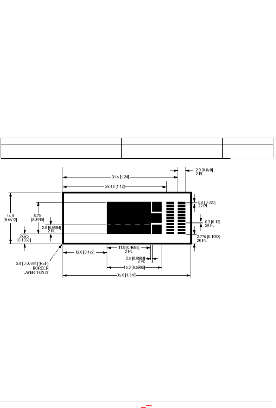
Table 4-1: Qualification Test Coupons
Test Type 1 Types 2,3,5 Types 4,6 Board
Physical Requirements
Plating Thickness M2, M5 M2, M5 M2, M5 X
IPC-2221 Test Speciman M, surface mount solderability testing, mm [in]
{EvaCombes: Please note, this drawing is designated IPC-2221-12-17}
4.2
4.3
Acceptance Tests
The sampling plan and frequency of acceptance testing except the solderability and plating thickness inspections
shall be in accordance with IPC-6011 and each sectional specification. The sampling plan of the solderability and
thickness of ENIG finish shall be as agreed upon by the user and the supplier (AABUS).
Quality Conformance Testing
Quality conformance testing shall consist of inspections as specified in IPC-6011 and each sectional specification,
with the addition of regular thickness inspections. The frequency of thickness inspection shall be 1 inspection (5
XRF measurements) per lot for Class 1 and 2, and as agreed upon by the user and the supplier (AABUS) for Class 3
products.
Page 6 of 2525
Download From http://bbs.infoeach.com
Download From http://bbs.infoeach.com

IPC-4552 Proposal June 2001
APPENDIX 1 CHEMICAL DEFINITIONS
Electroless Process
This chemical process promotes continuous deposition of a metal onto the PWB surface through an oxidation-
reduction chemical reaction, without the use of an external electrical potential. A reducing agent, such as sodium
hypophosphite, donates electrons to the positively charged metal ions in solution, thereby reducing the metal and
promoting its deposition onto the catalyzed metal surfaces of the PWB. This reaction is considered autocatalytic
because it will continue to plate in the presence of source metal ions and a reducing agent until the board is removed
from the plating bath. The thickness of plated deposits varies according to temperature, chemical parameters and the
amount of time spent in the plating bath.
Immersion Process
This chemical process uses a chemical displacement reaction to deposit a metal layer onto the exposed metal surface
of the PWB. In this reaction, the base metal donates the electrons that reduce the positively charged metal ions in the
solution. Driven by the electrochemical potential difference, the metal ions in solution (e.g., gold ions in the ENIG
process) are deposited onto the surface of the board, simultaneously displacing ions of the surface metal (e.g., nickel
ions in the ENIG process) back into solution. This reaction is considered self-limiting, because once the surface
metal is plated, there is no longer a source of electrons and the reaction stops
.
APPENDIX 2 PROCESS SEQUENCE
1. Cleaner
The purpose of this step is to clean the copper surface in preparation for processing. The cleaner removes oxides,
and light surface contaminants and ensures that the copper surface will be in a condition to be uniformly micro-
etched. Vendor specifications of temperature, dwell time, agitation and bath chemical control should be followed.
2. Microetch
The purpose of this step is to micro-etch the copper and to produce a surface that may be uniformly catalyzed and
plated with good deposit adhesion. A variety of different etchant types may be used (for example: sodium persulfate,
peroxide/sulfuric). Vendor specifications of temperature, dwell time, agitation and bath chemical control should be
followed.
3. Catalyst
The purpose of this step is to deposit a material that is catalytic to electroless nickel plating on the copper surface.
The catalyst lowers the activation energy for nickel deposition and allows plating to initiate on the copper surface.
Examples of catalysts include palladium and ruthenium. Vendor specifications of temperature, dwell time, agitation
and bath chemical control should be followed.
4. Electroless Nickel
The purpose of this bath is to deposit the required thickness of electroless nickel on the catalyzed copper surface.
The nickel thickness should be adequate to create a diffusion barrier to copper migration, and also to serve as a
solderable surface depending on the intended application.
The nickel bath has a relatively high deposition rate and its active chemical components must be replenished and
maintained in balance on a continuous basis. Electroless nickel baths typically run at high temperatures and
extended dwell time to achieve the required deposit thickness. It is therefore important to ensure that compatible
PWB substrate and solder mask materials are used. Vendor specifications of temperature, dwell time, agitation, bath
loading and bath chemical control should be followed.
5. Immersion Gold
The purpose of this step is to deposit a thin continuous layer of immersion gold. The gold protects the electroless
nickel from oxidation or passivation, and also serves as a contact surface depending on the intended application.
This bath runs at relatively high temperatures and dwell times. Ensure compatibility of substrate and solder mask if
used. Vendor specifications of temperature, dwell time, agitation and bath chemical control should be followed.
Page 7 of 10
Download From http://bbs.infoeach.com
Download From http://bbs.infoeach.com