IPC-4552.pdf - 第9页
IPC-4552 Proposal June 2001 APPENDIX 1 CHEMICAL DEFINITIONS Electroless Process This chemical process promotes co ntinuous deposition of a metal onto th e PWB surface through an oxidation- reduction chemical reaction, w …
IPC-4552 Proposal June 2001
structures on the outer layers. This impact will be more prevalent when ENIG is applied over all copper
f
eatures,
such as application of ENIG before solder mask. This impact is minimized when only the pads (not the traces) are
plated with the finish.
4
QUALITY ASSURANCE PROVISIONS
General Quality Assurance Provisions are specified in IPC-6011 and each sectional specification. Additional
requirements for PWB with electroless nickel/immersion gold (ENIG) plating are specified herein for qualification,
acceptance and quality conformance.
4.1
4.1.1
Qualification
Qualification of a PWB product is agreed upon by the user and supplier (see IPC-6011). The process capability of a
supplier of PWB with ENIG finish shall be evaluated. APPENDIX 3 describes recommended qualification aspects
of the ENIG process by a PWB supplier.
Sample Test Coupons
Test specimens used for qualification of PWB with ENIG finish shall be as specified in IPC-2221 and each sectional
specification. Specimen for additional testing requirements is listed in Table 4-1.
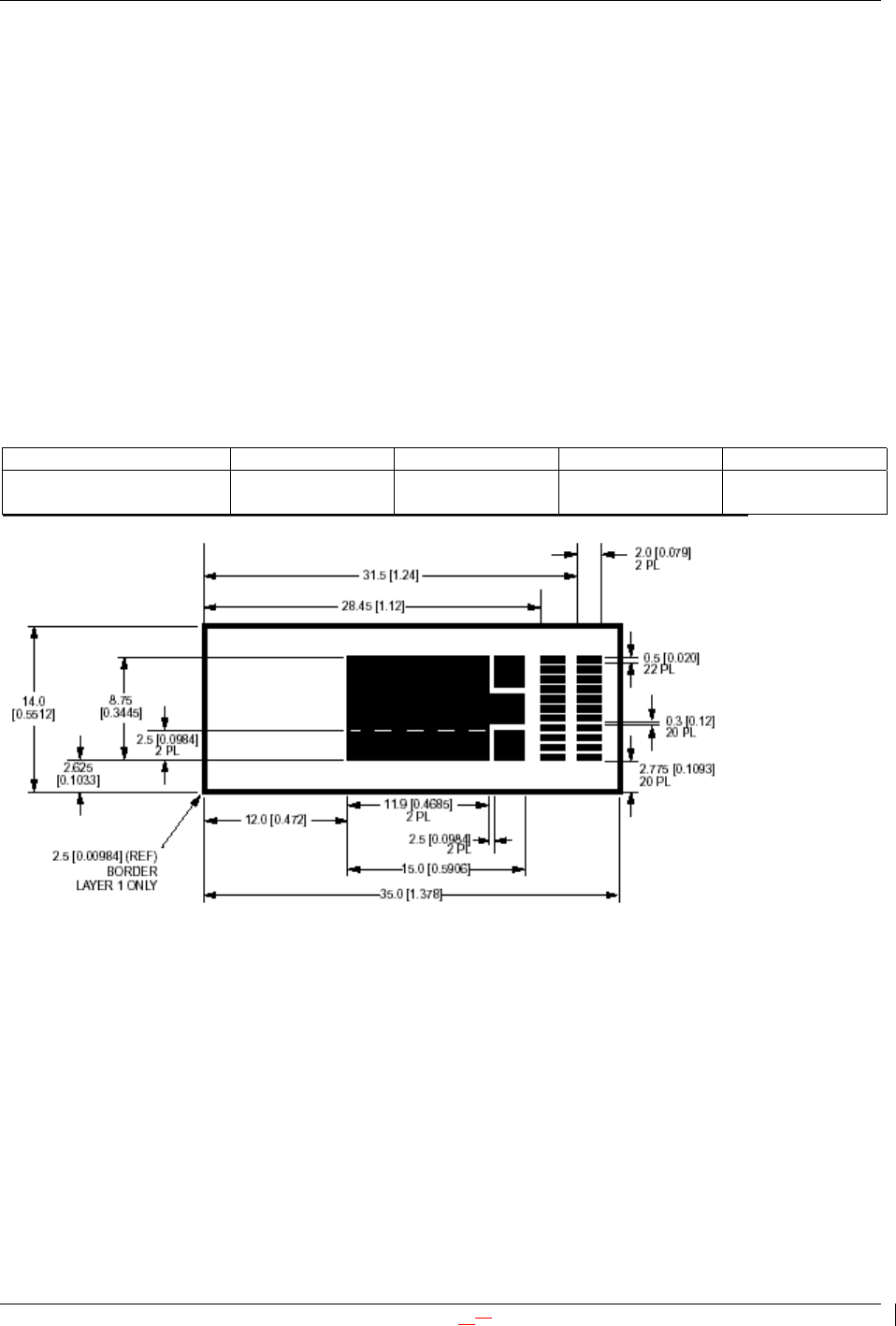
Table 4-1: Qualification Test Coupons
Test Type 1 Types 2,3,5 Types 4,6 Board
Physical Requirements
Plating Thickness M2, M5 M2, M5 M2, M5 X
IPC-2221 Test Speciman M, surface mount solderability testing, mm [in]
{EvaCombes: Please note, this drawing is designated IPC-2221-12-17}
4.2
4.3
Acceptance Tests
The sampling plan and frequency of acceptance testing except the solderability and plating thickness inspections
shall be in accordance with IPC-6011 and each sectional specification. The sampling plan of the solderability and
thickness of ENIG finish shall be as agreed upon by the user and the supplier (AABUS).
Quality Conformance Testing
Quality conformance testing shall consist of inspections as specified in IPC-6011 and each sectional specification,
with the addition of regular thickness inspections. The frequency of thickness inspection shall be 1 inspection (5
XRF measurements) per lot for Class 1 and 2, and as agreed upon by the user and the supplier (AABUS) for Class 3
products.
Page 6 of 2525
Download From http://bbs.infoeach.com
Download From http://bbs.infoeach.com

IPC-4552 Proposal June 2001
APPENDIX 1 CHEMICAL DEFINITIONS
Electroless Process
This chemical process promotes continuous deposition of a metal onto the PWB surface through an oxidation-
reduction chemical reaction, without the use of an external electrical potential. A reducing agent, such as sodium
hypophosphite, donates electrons to the positively charged metal ions in solution, thereby reducing the metal and
promoting its deposition onto the catalyzed metal surfaces of the PWB. This reaction is considered autocatalytic
because it will continue to plate in the presence of source metal ions and a reducing agent until the board is removed
from the plating bath. The thickness of plated deposits varies according to temperature, chemical parameters and the
amount of time spent in the plating bath.
Immersion Process
This chemical process uses a chemical displacement reaction to deposit a metal layer onto the exposed metal surface
of the PWB. In this reaction, the base metal donates the electrons that reduce the positively charged metal ions in the
solution. Driven by the electrochemical potential difference, the metal ions in solution (e.g., gold ions in the ENIG
process) are deposited onto the surface of the board, simultaneously displacing ions of the surface metal (e.g., nickel
ions in the ENIG process) back into solution. This reaction is considered self-limiting, because once the surface
metal is plated, there is no longer a source of electrons and the reaction stops
.
APPENDIX 2 PROCESS SEQUENCE
1. Cleaner
The purpose of this step is to clean the copper surface in preparation for processing. The cleaner removes oxides,
and light surface contaminants and ensures that the copper surface will be in a condition to be uniformly micro-
etched. Vendor specifications of temperature, dwell time, agitation and bath chemical control should be followed.
2. Microetch
The purpose of this step is to micro-etch the copper and to produce a surface that may be uniformly catalyzed and
plated with good deposit adhesion. A variety of different etchant types may be used (for example: sodium persulfate,
peroxide/sulfuric). Vendor specifications of temperature, dwell time, agitation and bath chemical control should be
followed.
3. Catalyst
The purpose of this step is to deposit a material that is catalytic to electroless nickel plating on the copper surface.
The catalyst lowers the activation energy for nickel deposition and allows plating to initiate on the copper surface.
Examples of catalysts include palladium and ruthenium. Vendor specifications of temperature, dwell time, agitation
and bath chemical control should be followed.
4. Electroless Nickel
The purpose of this bath is to deposit the required thickness of electroless nickel on the catalyzed copper surface.
The nickel thickness should be adequate to create a diffusion barrier to copper migration, and also to serve as a
solderable surface depending on the intended application.
The nickel bath has a relatively high deposition rate and its active chemical components must be replenished and
maintained in balance on a continuous basis. Electroless nickel baths typically run at high temperatures and
extended dwell time to achieve the required deposit thickness. It is therefore important to ensure that compatible
PWB substrate and solder mask materials are used. Vendor specifications of temperature, dwell time, agitation, bath
loading and bath chemical control should be followed.
5. Immersion Gold
The purpose of this step is to deposit a thin continuous layer of immersion gold. The gold protects the electroless
nickel from oxidation or passivation, and also serves as a contact surface depending on the intended application.
This bath runs at relatively high temperatures and dwell times. Ensure compatibility of substrate and solder mask if
used. Vendor specifications of temperature, dwell time, agitation and bath chemical control should be followed.
Page 7 of 10
Download From http://bbs.infoeach.com
Download From http://bbs.infoeach.com

IPC-4552 Proposal June 2001
6. Rinsing
The purpose of this step is to remove residual process chemicals from the PWB surface after each chemical
processing step. This may be achieved in a single or multiple rinse steps. In some instances pre-dip and/or post-dip
process steps may also be required for optimum process performance. Vendor specifications of temperature, dwell
time, agitation and turn over rate should be followed.
7. Drying
The purpose of this step is to ensure the boards are completely dry. This may be achieved by online vertical or off
line horizontal drying. Offline horizontal drying should be preceded by a horizontal rinsing step and should be
dedicated to the ENIG process. The time and temperature have to be optimized to suit the type of product.
APPENDIX 3 Qualification of ENIG Process by the Board Supplier
During process qualification, the following aspects shall be required:
Solderabilty
Solderability shall meet the requirements of J-STD-003 Category 3 throughout the life of the nickel bath.
Thickness Distribution
Characterize thickness distribution from panel to panel and within the different features of the panel. Establish
acceptance criteria.
Compatibility
Due to the chemically aggressive nature of the ENIG process, verification of material compatibility is very
important. Verify that the process is compatible with pre- and with post-process steps and material. Solder
mask/legend ink are good example of process or material compatibility concerns.
Processability
Follow vendor instructions for process control to include; temperature/dwell time, frequency of analysis, dump and
remake schedules, controllers etc. The use of automatic controllers for the nickel bath is a must for production
facilities.
APPENDIX 4 Recommendation For Thickness Measurement
General recommendations for accurately measuring the thickness of ENIG on copper clad epoxy laminate,
(Au/Ni/Cu/epoxy) using Energy Dispersive X-ray Fluorescence (EDS-XRF) are as follows. Contact your XRF
supplier for compliance with these recommendations or other specific procedures.
Standards
The measured thickness value for the standard should match the labeled, NIST-traceable value, to within 5% for the
top layer (Au) and 10% for the second layer (Ni). A minimum of one thickness standard should be measured at the
same time as the sample lot. Choose a standard that is close to the expected thickness to be measured. For the most
accurate results, the standard should match the base material of the sample.
Beam Size
The size of the X-ray beam should be at least 30% smaller than the area of the samples measured. Larger beam sizes
could give erroneous higher thickness values for Au. This is a result of interference from the Br in the base material.
Energy Range (Spectral Line)
The energy range or spectral line associated with Au must be carefully selected to avoid overlap from the Cu layer
line and from the Br line in the epoxy laminate. EDS-XRF instruments with solid-state detector typically do not
have overlap issues, and can measure Au using the Au L spectral line. Pin Diode Detector instruments have a small
overlap between the bromine (Br) K spectral line and the Au L line. To avoid Br interference use the Au L line from
9.4 KeV to 10.1 KeV, for the measurement. Gas Proportional Counters, have overlap both between the copper (Cu)
K line and the Au L line and between the Au L line and the Br K line. Select the Au L line from 10.5 KeV to 12.7
Page 8 of 10
Download From http://bbs.infoeach.com
Download From http://bbs.infoeach.com