JUKI_KE-3010A_MAINTE_CH.pdf - 第262页
Maintena nce Guide 14 - 16 14 -3- 5. ETHER - MAIN Board ( 40149647 ) [Functions] This ET HER - MAIN board is a ho st board used to communicate with the ETHER - SLAVE board through the Ethernet. The board is connected to …
维修调整要领书
14-13
14-3-4.
IEEE1394
基板(
40044519
)
【功能】
IEEE1394 BOARD 是与激光传感器 LNC60 之间的通信板。
经由 IEEE 1394a-2000 规格(也被称为 FireWire400)的通信,LNC60 与 CPU BOARD 之间进行
通信。
同时,还通过这一通信电缆向 LNC60 供给电源(DC+12V)。
制造制造商
制造商型号
ADLINK cPCI-8273JK/6U
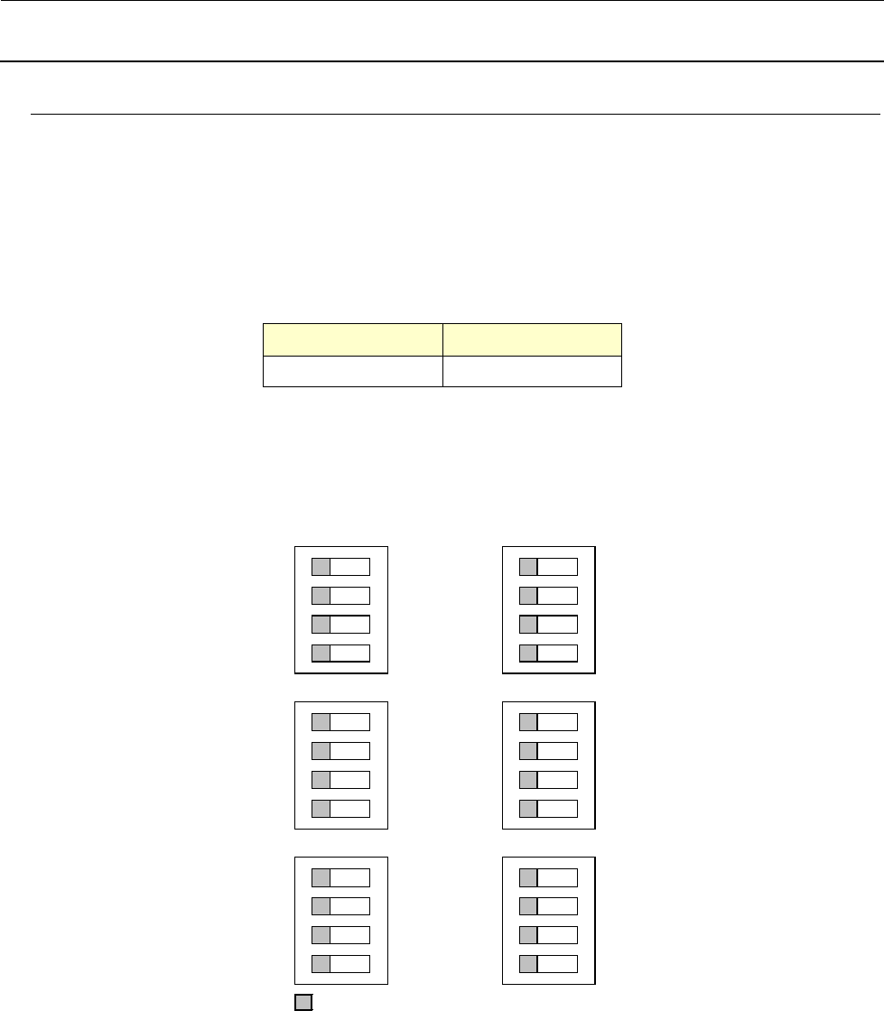
【双列开关的设定】
交货时已经设置好,在安装基板时请进行确认作业。
部がスイッチの設定位置
O N
1
2
3
4
S1
O N
1
2
3
4
S3
O N
1
2
3
4
S5
O N
1
2
3
4
S2
O N
1
2
3
4
S4
O N
1
2
3
4
S6
【LED 的意义】
IEEE1394 基板上没有 LED。
【更换后的调整项目】
没有特别需要调整的项目。
部表示开关的设置位置
Maintenance Guide
14-16
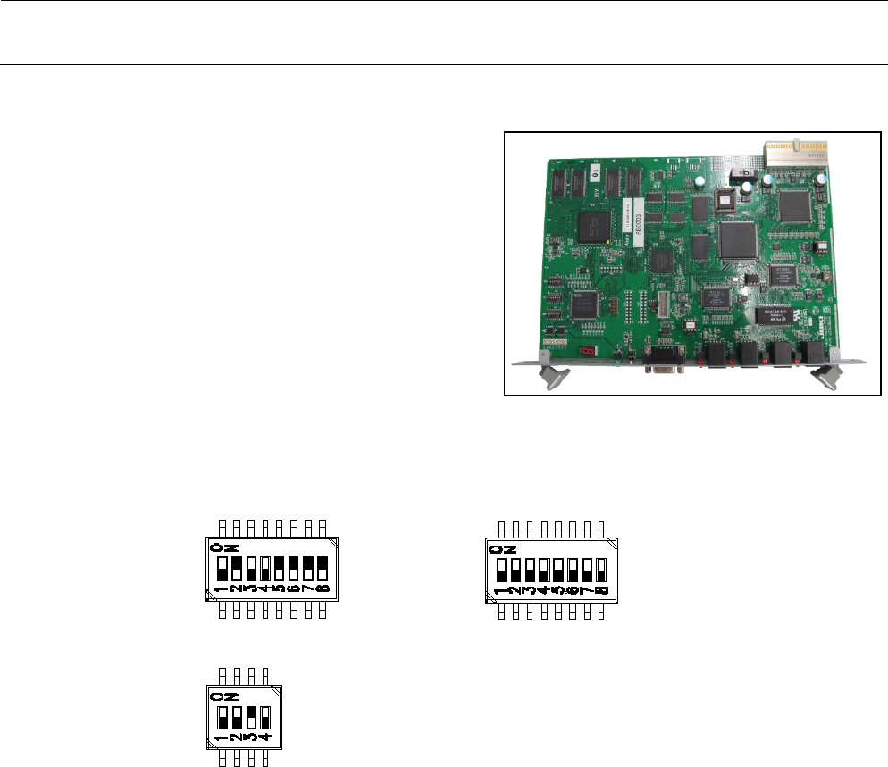
14-3-5. ETHER-MAIN Board (40149647)
[Functions]
This ETHER-MAIN board is a host board used
to communicate with the ETHER-SLAVE board
through the Ethernet.
The board is connected to the Compact PCI
(hereafter referred to as “cPCI”) bus so as to
access each peripheral I/O from the CPU board.
Additionally, the MS parameter backup data is
saved into the FLASH ROM.
[DIP-switch settings]
The DIP-switches have been set properly at the delivery of the machine. When setting the
board in the control unit, check the DIP-switch settings. ( portions show the switch
positions.)
Figure 14-3-5-1 DIP-Switches on ETHER-MAIN Board Assembly
[Meaning of LED]
7-segment LED: Shows the operation status of this board.
RUN LED: Lights up when the power is supplied.
EN1: Shows Link/Act of EN1. EN1 → Left station
EN2: Shows Link/Act of EN2. EN2 → Right station
EN3: Shows Link/Act of EN3. EN3 → S-XY-RELAY board – BASE CARRY board –
FEEDER board
EN4: Shows Link/Act of EN4.
[Adjustment items after replacement]
After that, follow the steps below to update the FLASH memory.
Select [Options] and [Change User Group], and then select [Serviceman].
Select [Maintenance] and [MS Parameter Setup].
Select [Upgrade] and [Ether Main].
Clicking [Exec.] will start the upgrading process.
Application management> Execute "SSD ====> Flash" from control data management
and back up the control data in the ETHER-MAIN board.
SW2-1 :OFF
SW2-2 :ON
SW2-3 :OFF
SW2-4 :OFF
SW2-5 :ON
SW2-6 :ON
SW2-7 :ON
SW2-8 :ON
SW4-1 :OFF
SW4-2 :OFF
SW4-3 :OFF
SW4-4 :OFF
SW4-5 :OFF
SW4-6 :OFF
SW4-7 :OFF
SW4-8 :OFF
SW1-1 :OFF
SW1-2 :OFF
SW1-3 :ON
SW1-4 :OFF
SW5:OFF
维修调整要领书
14-15
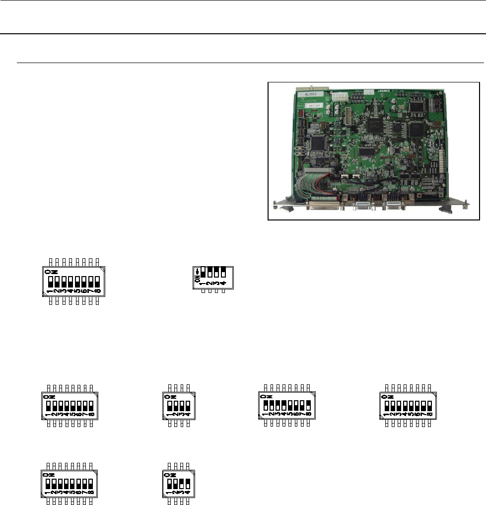
14-3-6.
IP-X7 BASE ASM
(
40071283
),
IP-X7 SUB ASM
(
40071293
)
【功能】
此基板是处理用 OCC 摄像头拍取的基板标记、IC
标记等图象数据,计算出基板位置矫正、零件位置
矫正所需要的值的图象处理基板。
【双列开关的设定】
双列开关在购入时,已经进行了设定,但在控制装置上安装基板时,请进行确认操作。(■部表示开
关的位置。)
※ SW2 是钢琴型,通过前面板侧进行操作。
图
14-3-6-1 IP-X7BASE
组
DIP-SW
图
14-3-6-2 IP-X7SUB
组
DIP-SW
【前面板开关】 ※ 这些开关,一般请不要进行操作。
重新设置 SW: 对此基板进行复位。
异常中断 SW: 对 CPU 发行 NMI。
双列开关: 变更基板的设定。
【更换后的调整项目】
请按照以下的程序,进行 FLASH 存储器的版本升级。
① 「选购品」 →「变更用户等级」,选择「维修人员」。
② 「维修」 → 请选择「MS 参数设定」。
③ 「版本升级」 → 请选择「图象」。
④ 单击「执行」,版本升级开始。
SW1-1 :OFF
SW1-2 :OFF
SW1-3 :OFF
SW1-4 :OFF
SW1-5 :OFF
SW1-6 :OFF
SW1-7 :OFF
SW1-8 :OFF
SW2-1 :ON
SW2-2 :OFF
SW2-3 :OFF
SW2-4 :OFF
SW2-1 :OFF
SW2-2 :OFF
SW2-3 :OFF
SW2-4 :OFF
SW1-1 :OFF
SW1-2 :OFF
SW1-3 :OFF
SW1-4 :OFF
SW1-5 :OFF
SW1-6 :OFF
SW1-7 :OFF
SW1-8 :OFF
SW3-1 :ON
SW3-2 :ON
SW3-3 :ON
SW3-4 :ON
SW3-5 :OFF
SW3-6 :OFF
SW3-7 :OFF
SW3-8 :ON
SW4-1 :OFF
SW4-2 :OFF
SW4-3 :OFF
SW4-4 :OFF
SW4-5 :OFF
SW4-6 :OFF
SW4-7 :OFF
SW4-8 :OFF
SW5-1 :OFF
SW5-2 :OFF
SW5-3 :OFF
SW5-4 :OFF
SW5-5 :OFF
SW5-6 :OFF
SW5-7 :OFF
SW5-8 :OFF
SW8-1 :OFF
SW8-2 :OFF
SW8-3 :ON
SW8-4 :ON