ASM_catalogue_ASM_Stencils_from_the_global_No_1_EN_210419.pdf - 第11页
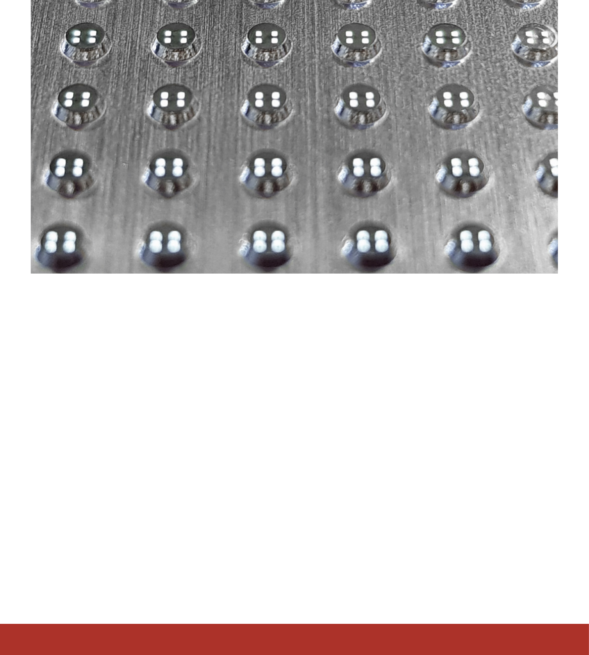
Electroform stencils can be produced with modications to accommodate specic applications. One such adaptation is a technique called V ariable Aperture Height T echnology (V AHT), whereby a gasket overgrowth is created …
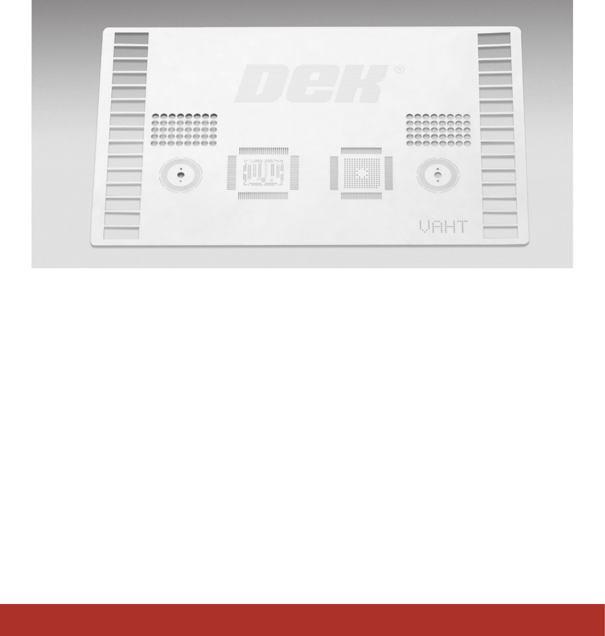
DEK Electroform 3D stencils
DEK Electroform 3D stencils ensure highest print quality and throughput for jobs
that require printing with different height levels and into indentations.
DEK Electroform 3D stencils are single thickness stencils
produced to accommodate mass imaging of surfaces that are
not at or include features or structures that would prohibit
conventional one-pass printing.
Well-suited for printing inside cavities or cover printing on pre-
populated substrates, 3D stencils allow higher throughput and
lower costs through the elimination of secondary printing or
dispensing steps.
Benets:
■ Enables single pass printing for challenging, non-flat or pre-
populated substrates
■ Lowers cost by eliminating traditional secondary printing or
dispensing steps used to accommodate positive or negative
Z axis values
■ Improves production throughput
■ Can be manufactured to conform to any shape or topography
■ Better uniformity and deposit shape control than with
dispensing processes
Specications:
■ Special, (usually) supplied slotted squeegee required
■ Proven for a variety of different applications
- LED cavity printing
- SMT multi-level printing
- SMT ceramic substrate cavity printing
- Semiconductor printing to accommodate wafer embossment
- Semiconductor die top printing
■ Stencil frame size: DEK VectorGuard
TM
Classic or
DEK VectorGuard
TM
High Tension 23” x 23” recommended
■ Stencil foil thickness: 50 µm - 250 µm (2 mil-10 mil)
■ Pocket size: 2.0 mm square (min)
■ Pocket depth: 2.0 mm (max, depending on pocket size)
■ Pocket to pocket gap allowance: 2.5 mm (min)
10
|
Process Support Products
|
ASM: Stencils from the global No. 1
Electroform stencils can be produced with modications to
accommodate specic applications. One such adaptation is a
technique called Variable Aperture Height Technology (VAHT),
whereby a gasket overgrowth is created around apertures to
create more aperture height to allow for increased paste volumes
to be deposited.
VAHT is ideal for PCBs that incorporate both small and large
components that require varying amounts of solder material.
Aperture gasket height can be 1 to 2 mils higher than the base
stencil thickness.
DEK Electroform Variable Aperture
Height Technology (VAHT)
DEK VAHT technology offers a unique alternative to multi-level stencils for non-
homogeneous assemblies that call for larger, area-specific paste volumes to
accommodate bigger components.
Benets:
■ Ideal for heterogeneous assemblies, allowing printing of
various solder paste volumes with a single stencil
■ Improved throughput
11
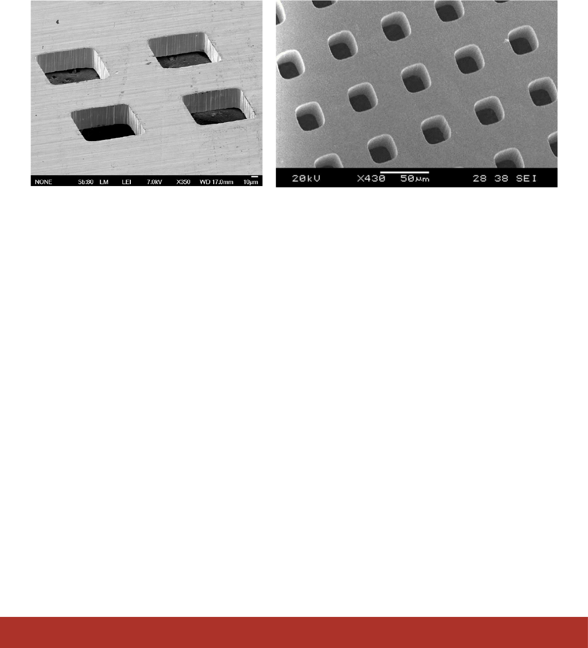
NEW: DEK Electroform
Mini LED Stencil
Miniaturization trend demands stencil with smaller apertures.
In recent years, miniLED has emerged as a new segment with
high growth potential and has drawn the interest of most major
LED companies. miniLED are used in the back-light units (BLUs)
of display screens and are very competitive both in terms of cost
and function, oering excellent contrast though the use of local
dimming. However, miniLED products pose a real problem to
the packaging industry which has not yet developed solutions
for handling such small dies with the accuracy and throughput
required; a typical miniLED die is smaller than an 0201m
component.
The challenges related to stencil printing for miniLED products
involve printing paste deposits which are smaller than 100µm
in size and controlling the uniformity of the paste deposits to
avoid die tilt, bridging and other defects. Electroform is uniquely
positioned to address these challenges. Electroformed stencils
have better paste release capabilities, a result of the superior
smoothness of the aperture side wall and the surface energy of
nickel.
In addition, miniLED products using RGB congurations typically
require more than 100,000 apertures in one stencil as well as a
stencil thickness in the range of 23 – 40 µm. Laser cut stencils
are not able to meet such requirements.
Specications:
■ Aperture Size: 40 µm × 40 µm (minimum), ± 5 µm
■ Thickness: 23 µm (minimum)
■ Gap between apertures: 50 µm (maximum)
■ Frame Size: DEK VectorGuard
TM
23” × 23”
■ Positional Accuracy: 0.1 µm/mm
12
|
Process Support Products
|
ASM: Stencils from the global No. 1