ASM_catalogue_ASM_Stencils_from_the_global_No_1_EN_210419.pdf - 第9页
3D printing Applications: ■ Semiconductor packaging - W afer and substrate bumping - Ball placement - Leadframe printing - Low-T emperature Co-fired Ceramics (L TCC) - Die attach ■ LED Printing - LED leadframe printing -…
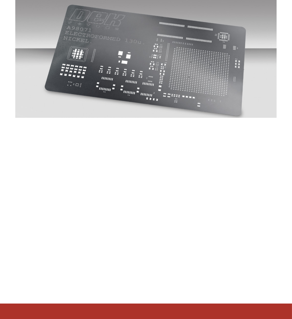
DEK Electroform solutions
Achieve ultimate material volume consistency control for standard
SMT, micro-SMT, semiconductor, solar and LED lighting applications with
DEK Electroform stencils.
Singapore Center of Competence
To develop new manufacturing processes such as electroplating
solutions for stencils, ASM operates a center of competence in
Singapore with its own nickel electroplating facility. The local
team has many years of experience and deep expertise in the
production of electroformed stencils and parts for non-SMT
components. The stencil designs are developed and tested in the
adjacent application center.
By providing maximum control over the thickness and evenness
of stencils, DEK’s electroforming technology ensures ultimate
consistency for many standard SMT, micro SMT, semiconductor,
solar and LED applications. With material thicknesses down to
12 microns, the material can be adapted to meet any current and
future requirements. In addition, electroforming technology oers
the possibility to manufacture specialized components in large
volumes, thus reducing their unit cost.
Made with an additive galvanic process, DEK Electroform
stencils can be produced with extremely complex designs to
enable the printing of exceptionally small deposits in recesses,
around components, or on multiple levels. In many applications,
electroformed stencils are clearly superior to stencils produced
with traditional dispensing or spray coating techniques by
delivering more throughput per hour and improved performance.
Features and benets:
■ Min thickness: 12 µm to 200 µm
■ Min stencil size:
DEK VectorGuard™ 432 mm × 432 mm (17” × 17”)
■ Max stencil size:
DEK VectorGuard™ 584 mm × 736 mm (23” × 29”)
DEK Mesh-mounted frame solution 736 mm × 736 mm
(29” × 29")
■ No additional costs for large quantities of apertures
■ No deformation of stencil like lasering of large quantities of
apertures like for wafer bumping
■ Test and development support for new projects
8
|
Process Support Products
|
ASM: Stencils from the global No. 1
3D printing
Applications:
■ Semiconductor packaging
- Wafer and substrate bumping
- Ball placement
- Leadframe printing
- Low-Temperature Co-fired Ceramics (LTCC)
- Die attach
■ LED Printing
- LED leadframe printing
- Flux printing for flip-chip mounting
- Phosphor layer printing on wafer die or over flip chip die
- Piece parts
■ 3D printing on wafers, substrates
■ Surface-mount assembly
- Standard SMT printing
- VAHT stencils – variable height on different apertures
- 3D stencils – print apertures on different levels; cover
components and print around the covered area
■ Piece Parts
- Electrical test probes
- Electro-mechanical parts
- Multiple other parts such as foils and sieves
9
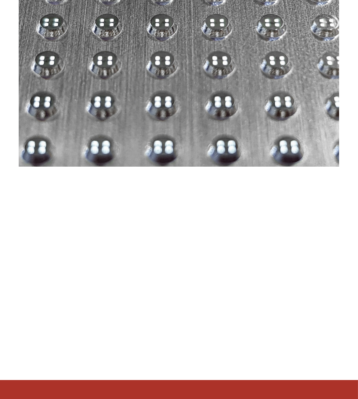
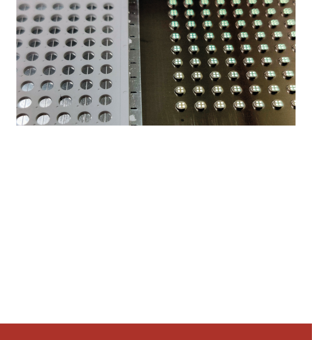
DEK Electroform 3D stencils
DEK Electroform 3D stencils ensure highest print quality and throughput for jobs
that require printing with different height levels and into indentations.
DEK Electroform 3D stencils are single thickness stencils
produced to accommodate mass imaging of surfaces that are
not at or include features or structures that would prohibit
conventional one-pass printing.
Well-suited for printing inside cavities or cover printing on pre-
populated substrates, 3D stencils allow higher throughput and
lower costs through the elimination of secondary printing or
dispensing steps.
Benets:
■ Enables single pass printing for challenging, non-flat or pre-
populated substrates
■ Lowers cost by eliminating traditional secondary printing or
dispensing steps used to accommodate positive or negative
Z axis values
■ Improves production throughput
■ Can be manufactured to conform to any shape or topography
■ Better uniformity and deposit shape control than with
dispensing processes
Specications:
■ Special, (usually) supplied slotted squeegee required
■ Proven for a variety of different applications
- LED cavity printing
- SMT multi-level printing
- SMT ceramic substrate cavity printing
- Semiconductor printing to accommodate wafer embossment
- Semiconductor die top printing
■ Stencil frame size: DEK VectorGuard
TM
Classic or
DEK VectorGuard
TM
High Tension 23” x 23” recommended
■ Stencil foil thickness: 50 µm - 250 µm (2 mil-10 mil)
■ Pocket size: 2.0 mm square (min)
■ Pocket depth: 2.0 mm (max, depending on pocket size)
■ Pocket to pocket gap allowance: 2.5 mm (min)
10
|
Process Support Products
|
ASM: Stencils from the global No. 1