ASM_catalogue_ASM_Stencils_from_the_global_No_1_EN_210419.pdf - 第7页
ASM LASER CUT STENCIL Standard stainless steel Laser cut nickel Fine grain stainless steel Standard E-form nickel Platinum E-form stencil Material type 304 PHD Nickel Fine grain SS Hard nickel Hard nickel Material hardne…
DEK Fine Grain stencils
DEK Fine Grain stencils can be used with the DEK Mesh-
mounted frames, DEK VectorGuard
TM
Classic and DEK
VectorGuard
TM
High Tension frame systems. Fine grain stainless
steel stencils provide smoother laser-cut aperture walls for
improved paste release and better material transfer efficiency.
A cost-effective alternative to nickel, fine grain stainless steel is
ideal for challenging dimensions and high-density assemblies.
Achieving a finer grain of stainless steel, DEK Fine Grain stencils
provide superior paste release and a smoother stencil surface.
DEK Stencil solutions – stencil
technical specification
ASM LASER CUT STENCIL
Standard stainless
steel
Laser cut nickel Fine grain stainless
steel
Standard
E-form nickel
Platinum
E-form stencil
Material type 304 PHD
Nickel Fine grain SS Hard nickel Hard nickel
Material hardness (HV) ≥370 >470+ ≥370 500 +/-50 500 +/-50
Grain size (µm) 16-25 1 ≤ 2 1 0.6
Thickness available (µm) 80-250 100-175 80-250 75- 200 20-230
Thickness tolerance 4% 7% <2% 10% <5%
Area ratio window >0.66 >0.6 >0.55 >0.5 >0.5
Sheet width max 690 mm 584 mm 610 mm 610 mm 584 mm
Apertures size tolerance ±5 µm ±5 µm ±5 µm ±10 µm ±4 µm
6
|
Process Support Products
|
ASM: Stencils from the global No. 1
ASM LASER CUT STENCIL
Standard stainless
steel
Laser cut nickel Fine grain stainless
steel
Standard
E-form nickel
Platinum
E-form stencil
Material type 304 PHD
Nickel Fine grain SS Hard nickel Hard nickel
Material hardness (HV) ≥370 >470+ ≥370 500 +/-50 500 +/-50
Grain size (µm) 16-25 1 ≤ 2 1 0.6
Thickness available (µm) 80-250 100-175 80-250 75- 200 20-230
Thickness tolerance 4% 7% <2% 10% <5%
Area ratio window >0.66 >0.6 >0.55 >0.5 >0.5
Sheet width max 690 mm 584 mm 610 mm 610 mm 584 mm
Apertures size tolerance ±5 µm ±5 µm ±5 µm ±10 µm ±4 µm
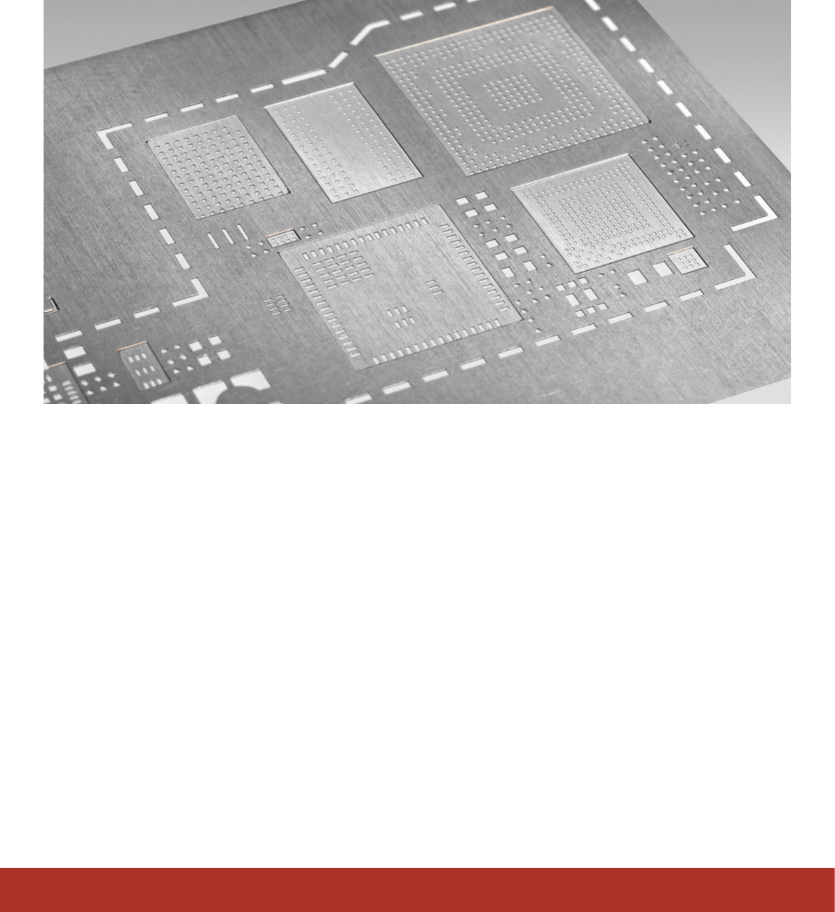
DEK Multi-level stencils
Ideal for ensuring optimized solder paste height and volume for components that are
distributed over a wide area, DEK Multi-level (step) stencils are produced with the latest
micro-milling technology to ensure exceptional accuracy and repeatability.
DEK Multi-level (step) stencils are available in stainless steel
or nickel and are ideal for printing paste on SMT boards with
ne pitch parts arranged over a large area. These stencils
provide excellent print performance for applications with micro
BGAs,
0.3 mm QFPs and small components such as 0201s metric, as
well as packaging applications and release of specialty solder
paste formulations
Multi-level stencils are available mesh mounted onto industry-
standard frames and are available for the DEK VectorGuard™
Classic and DEK VectorGuard
TM
High Tension frame systems.
Benets:
■ Flexible local adaptation to any component mix
■ Maximum positioning accuracy
■ Improved solder paste homogeneity
■ Improved repeat accuracy thanks to extra-smooth surface
structure and high-precision edges
■ Minimized paste wastage through optimized surface structure
■ Significant reduction of paste residue in shadow areas
■ Flexible design of pressure-sensitive areas
■ Significant squeegee pressure reduction thanks to a modified
ramp profile
7
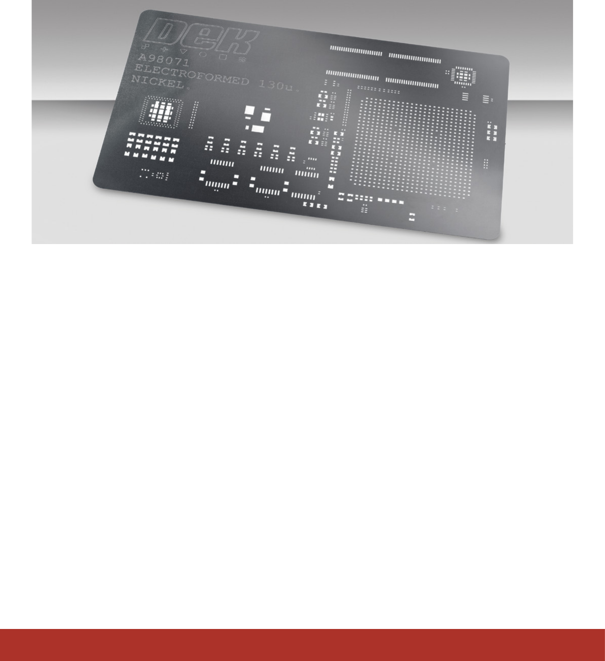
DEK Electroform solutions
Achieve ultimate material volume consistency control for standard
SMT, micro-SMT, semiconductor, solar and LED lighting applications with
DEK Electroform stencils.
Singapore Center of Competence
To develop new manufacturing processes such as electroplating
solutions for stencils, ASM operates a center of competence in
Singapore with its own nickel electroplating facility. The local
team has many years of experience and deep expertise in the
production of electroformed stencils and parts for non-SMT
components. The stencil designs are developed and tested in the
adjacent application center.
By providing maximum control over the thickness and evenness
of stencils, DEK’s electroforming technology ensures ultimate
consistency for many standard SMT, micro SMT, semiconductor,
solar and LED applications. With material thicknesses down to
12 microns, the material can be adapted to meet any current and
future requirements. In addition, electroforming technology oers
the possibility to manufacture specialized components in large
volumes, thus reducing their unit cost.
Made with an additive galvanic process, DEK Electroform
stencils can be produced with extremely complex designs to
enable the printing of exceptionally small deposits in recesses,
around components, or on multiple levels. In many applications,
electroformed stencils are clearly superior to stencils produced
with traditional dispensing or spray coating techniques by
delivering more throughput per hour and improved performance.
Features and benets:
■ Min thickness: 12 µm to 200 µm
■ Min stencil size:
DEK VectorGuard™ 432 mm × 432 mm (17” × 17”)
■ Max stencil size:
DEK VectorGuard™ 584 mm × 736 mm (23” × 29”)
DEK Mesh-mounted frame solution 736 mm × 736 mm
(29” × 29")
■ No additional costs for large quantities of apertures
■ No deformation of stencil like lasering of large quantities of
apertures like for wafer bumping
■ Test and development support for new projects
8
|
Process Support Products
|
ASM: Stencils from the global No. 1