ASM_catalogue_ASM_Stencils_from_the_global_No_1_EN_210419.pdf - 第13页
DEK PumpPrint™ / Adhesive stencils DEK PumpPrint TM technology enables a wide range of adhesive patterns to be successfully deposited using a screen printing platform. DEK PumpPrint TM / Adhesive stencils enable depositi…
NEW: DEK Electroform
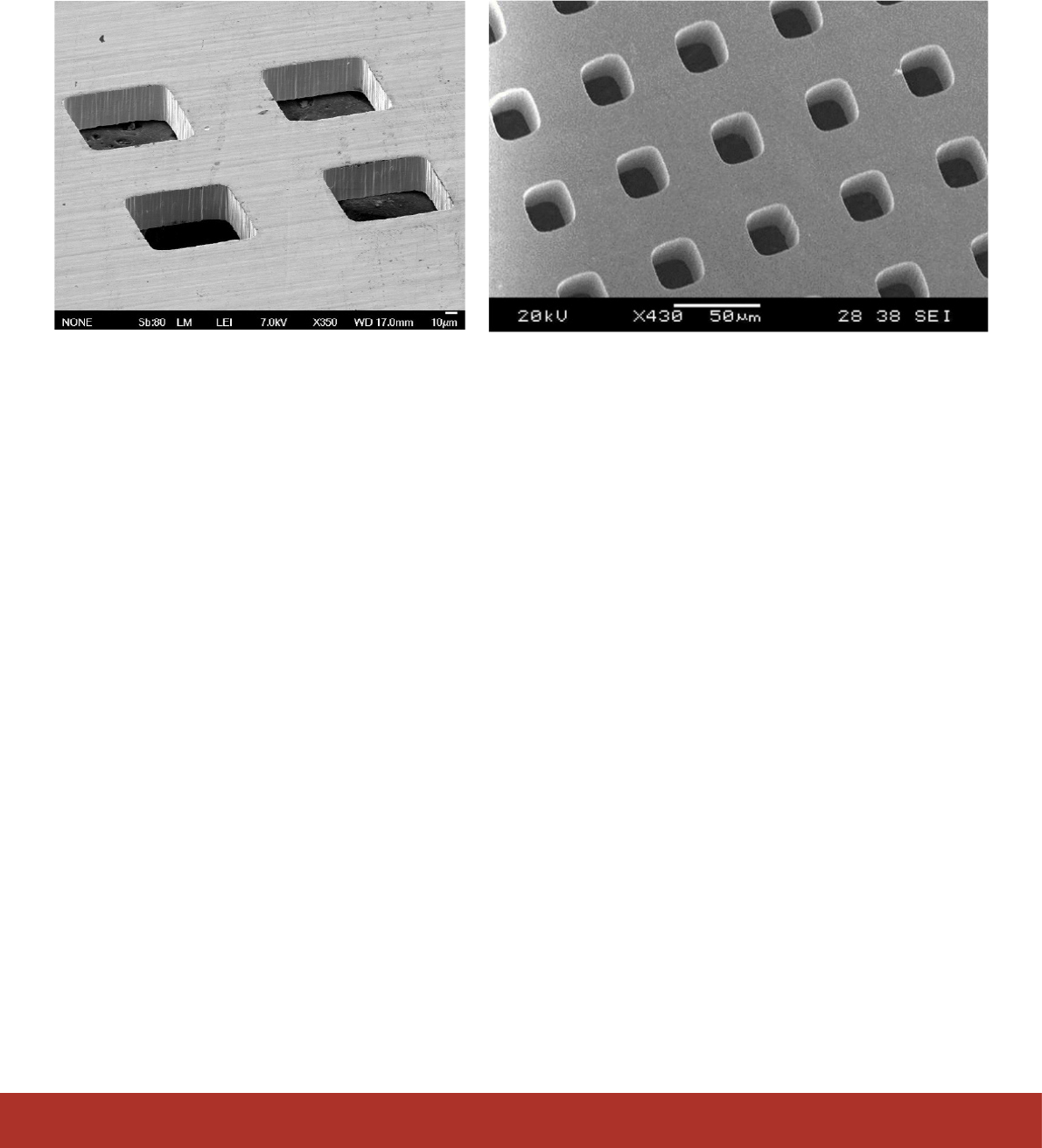
Mini LED Stencil
Miniaturization trend demands stencil with smaller apertures.
In recent years, miniLED has emerged as a new segment with
high growth potential and has drawn the interest of most major
LED companies. miniLED are used in the back-light units (BLUs)
of display screens and are very competitive both in terms of cost
and function, oering excellent contrast though the use of local
dimming. However, miniLED products pose a real problem to
the packaging industry which has not yet developed solutions
for handling such small dies with the accuracy and throughput
required; a typical miniLED die is smaller than an 0201m
component.
The challenges related to stencil printing for miniLED products
involve printing paste deposits which are smaller than 100µm
in size and controlling the uniformity of the paste deposits to
avoid die tilt, bridging and other defects. Electroform is uniquely
positioned to address these challenges. Electroformed stencils
have better paste release capabilities, a result of the superior
smoothness of the aperture side wall and the surface energy of
nickel.
In addition, miniLED products using RGB congurations typically
require more than 100,000 apertures in one stencil as well as a
stencil thickness in the range of 23 – 40 µm. Laser cut stencils
are not able to meet such requirements.
Specications:
■ Aperture Size: 40 µm × 40 µm (minimum), ± 5 µm
■ Thickness: 23 µm (minimum)
■ Gap between apertures: 50 µm (maximum)
■ Frame Size: DEK VectorGuard
TM
23” × 23”
■ Positional Accuracy: 0.1 µm/mm
12
|
Process Support Products
|
ASM: Stencils from the global No. 1
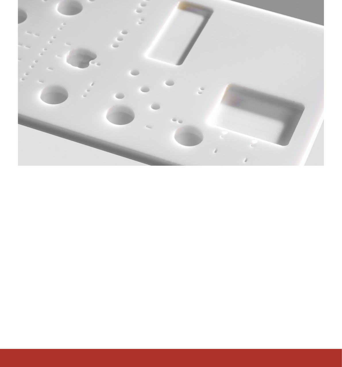
DEK PumpPrint™ /
Adhesive stencils
DEK PumpPrint
TM
technology enables a wide range of adhesive patterns to
be successfully deposited using a screen printing platform.
DEK PumpPrint
TM
/ Adhesive stencils enable deposition of
adhesives in a single stroke, as opposed to the slower, serial
process of dot dispensing systems. With adhesive printing,
throughput is dramatically increased and cycle time is constant.
Also eective for certain solder applications, DEK PumpPrint
TM
stencils can be utilized for solder deposition around through-hole
component leads or into the base of deep packages.
DEK PumpPrint
TM
/ Adhesive stencils are constructed of an
acrylic material and available in standard thicknesses of 1.0
mm to 3.0 mm, or up to 8 mm for special applications. Printing
through accurately machined apertures, deposit heights from
75 µm to 1 mm can be achieved. Specially designed DEK
PumpPrint
TM
stencils are also available for use with the DEK
VectorGuard
TM
Classic stencil frame system.
Features and benets:
■ Significantly improved throughput, efficiency, and flexibility
compared to traditional adhesive dispensing
■ Nozzle changeovers eliminated
■ Allows re-deployment of existing resources
■ Underside routing clears components, cut and clinched
through-hole leads, paste and solder mask
■ Stencils are lightweight and solvent-resistant
■ Available for the DEK VectorGuard
TM
Classic stencil frame
system
13
DEK NanoUltra stencil coating
Benets:
■ Coating applied to the bottom surface of the
stencil and to the aperture walls for optimized print
performance
■ Significantly reduces understencil cleaning
frequency requirements, lowering costs and
improving throughput
■ Delivers superior print definition for area ratios
below 0.6
■ Increases transfer efficiency by 10% to 40%
depending on area ratio
■ Reduces solder paste bridging
■ Encourages more uniform solder paste deposits
■ Colored coating provides visual confirmation of
coverage, as opposed to clear wipe-on nano
coatings
■ Micron-thick coating lasts longer compared to
wipe-on nano solutions
■ Non-ionic, not conductive, and chemically inert
■ ECHA REACH, RoHS and RoHS 2 compliance
■ Recommended stencil materials: Fine Grain and
stainless steel
TECHNICAL SPECIFICATIONS
Properties Values
Appearance Gold or red
Thickness of coating 2 to 4 micron
Specific gravity @ 25C 1.5 g/cm
3
Static contact angle, water 103 - 105°
Static contact angle, n-hexadecane 62 - 64°
Abrasion resistance, ASTM D2486, isopropyl alcohol > 2000 cycles
Abrasion resistance, ASTM D2486, IPA based flux > 2000 cycles
Pencil hardness > 9 H
Resistivity > 10 x 10
12
ohm-M
Ionic residues (ROSE) 0 μg of NaCl / liter
Ionic species on board (as received) None detected
Ionic species on board (after reflow) None detected
Applied upon completion of the stencil manufacturing process, DEK NanoUltra
fluxophobic stencil coatings deliver stencil underside and aperture coating
for maximum material transfer efficiency and optimized understencil cleaning
performance.
DEK NanoUltra STENCIL COATING
Part number Description
SAP DEK
03137311 800109 Europe
03137312 800110 Americas
14
|
Process Support Products
|
ASM: Stencils from the global No. 1