X-Serie S_705.pdf - 第47页
47 Vision sensor technology PCB position recognition Description The optimum fiducial sh apes vary accordi ng to the condi- tion of the surface. Wh en using b are copper surfac es with low oxidation, it is advis- able to…
46
Digital SIPLACE Vision system
Checking the component quality
Overview of key functions
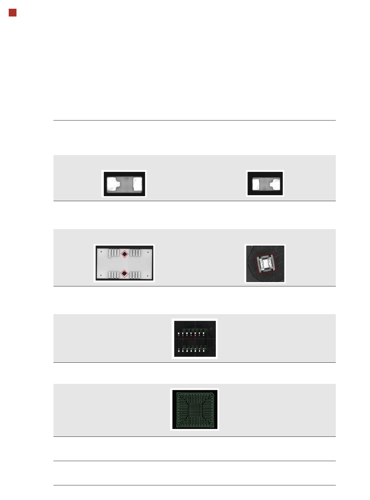
Checking the lead length
The lead length check determines whether the leads have been distorted. This inspection is possible by checking
whether leads of the same type e.g. chip shapes have different lengths. Flipped and rotated components can also
be detected.
Component OK in this position Rotated
Detecting special shapes with rectangular functions
When using certain special component shapes, it is sometimes necessary to program parts on the components or
outlines as rectangular shapes. This ensures that they can be processed more reliably.
Rectangular function on the component Rectangular component with irregular edges
Detecting incorrect component descriptions
The Vision system checks whether the position of the component corresponds to the measured Vision data. The
following example has more leads than were programmed in the component shape description.
Teaching complex BGA structures
Complex BGA structures can be taught within only a few seconds.
Placing when inkspot is not present
A fiducial can now be defined for the omission of panels. If a fiducial is found (cross, circle, etc.), this panel will be
omitted.
Checking the inner area of circular fiducials
To differentiate circular fiducials from other structures on the board, a brightness check is performed in the inner
area of these fiducials.

47
Vision sensor technology
PCB position recognition
Description
The optimum fiducial shapes
vary according to the condi-
tion of the surface. When
using bare copper surfaces
with low oxidation, it is advis-
able to take the single cross,
as the high amount of infor-
mation provided helps
achieve the greatest
accuracy. Rectangle, square
and circle are less "informa-
tive" but save space and can
even be used when oxidation
is at an advanced stage. Cir-
cle or square are advisable
for tin-plated structures as
the ratio of the fiducial
dimensions to the presolder
thickness is particularly
favorable.
Fiducial criteria
Locate 2 fiducials
Locate 3 fiducials
X-/Y-position, rotation angle, mean PCB distortion
additional: shearing, distortion separately in X and Y direc-
tion
Fiducial shapes Synthetic fiducials: circle, cross, square, rectangle, dia-
mond, circular, square and rectangular contours, double
cross, pattern: any
Fiducial surface
Copper
Tin
Without oxidation and solder resist
Warpage of fiducial 1/10 of structure width, both with good
contrast to environment
Dimensions of patterns
min. size
max. size
0.5 mm
3 mm
Fiducial environment Clearance around reference fiducial not necessary if there
is no similar fiducial structure in the search area
Dimensions of synthetic fiducials
Min. X/Y size for circle and rectangle 0.25 mm
Min. X/Y size for annulus and rectangle 0.3 mm
Min. X/Y size for cross 0.3 mm
Min. X/Y size for double cross 0.5 mm
Min. X/Y size for diamond 0.35 mm
Min. frame width for annulus and rectangle 0.1 mm
Min. bar width / bar distance for cross, double-cross 0.1 mm
Max. X/Y size for all fiducial shapes 3 mm
Max. bar width for cross/double-cross 1.5 mm
Minimum tolerances generally 2% of nominal dimension
Max. tolerances generally 20% of nominal dimension

48
Vision sensor technology
PCB position recognition
Bad board recognition
Ink spot criteria
Methods • Synthetic fiducial recognition method
• Mean gray scale value
• Histogram method
• Template matching
Shapes and sizes of fiducials/structures for
synthetic fiducials
other methods
For dimensions of synthetic fiducials, see page
47
min. 0.3 mm
max. 5 mm
Masking material Good coverage
Recognition time Depends on the method: 20 ms - 200ms
Description
In the cluster technology
each subpanel is assigned
an inkspot. If this is present
during the measurement via
the PCB vision module, the
corresponding subpanel is
populated. This function
helps prevent unnecessary
costs caused by placement
of defective panels.
Technical data for PCB position detection
PCB fiducials
Local fiducials
Library of bad panel recognition
Up to 3 (subpanels and multiple panels)
Up to 6 for the long board option (optional PCB fiducials
are output by the optimization.)
Up to 2 per PCB (may be of different type)
Up to 255 fiducial types per subpanel
Image analysis Edge detection method (singular feature) based on gray
scale values
Illumination type Front lighting
Fiducial recognition time 0.1 s
Field of vision 5.78 mm x 5.78 mm
Virtual inkspot handler (option)
The virtual inkspot handler allows you to scan in inkspots from an external system. These ink-
spots can then be allocated to the relevant board.