presentazione_laboratorio.pdf - 第3页
Low temperature Wafer Bonding MEMS Technological fabrication modules Silicon anisotropic etching with TMAH solution Composite suspended membranes Lithography with thick film of photoresist Gold Electrodeposition
MIS Microsystems
Head of Department: Mario Zen
The department designs and realises silicon
microsystems, especially:
• silicon particle detectors;
• sensors for bio-medical and environmental
applications;
• micro-electro-mechanic systems (MEMS) for
industrial and consumer applications;
• electro-optic microsystems for vision and non-
destructive measurements.
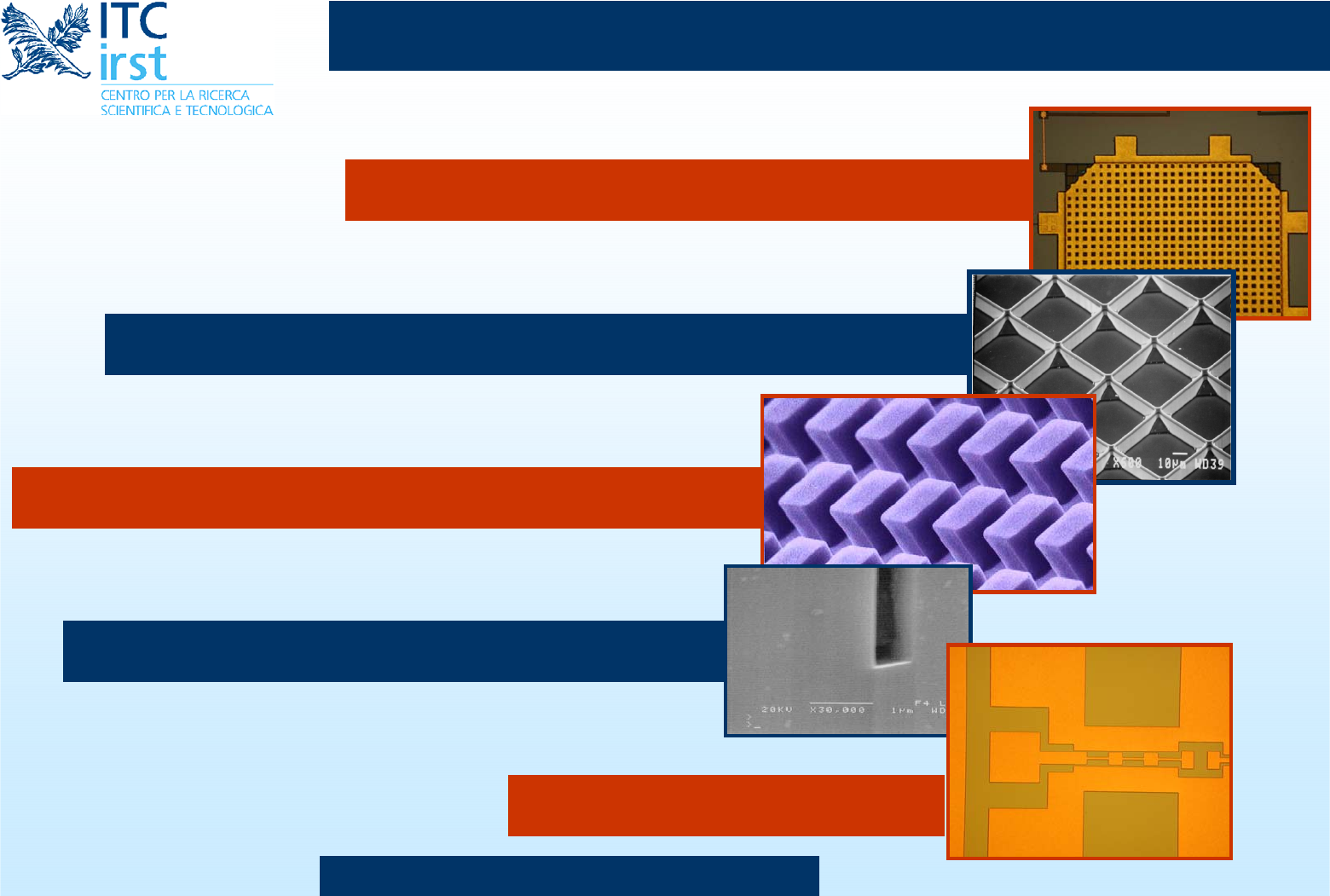
Low temperature Wafer Bonding
MEMS Technological fabrication modules
Silicon anisotropic etching with TMAH solution
Composite suspended membranes
Lithography with thick film of photoresist
Gold Electrodeposition

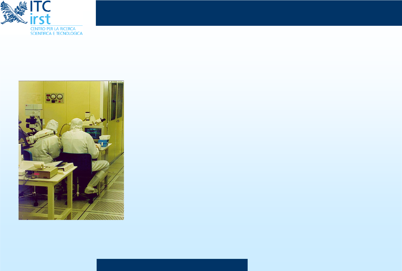
Clean Room
Fabrication: the Lab. covers an area of 500 sqm (250 of
which are in class 10)
• Furnaces 11 horizontal furnaces (diffusion,LPCVD depositions, Si3N4,
Polysilicon, TEOS, BPSG and LTO)
• Implanter “Varian E 220 medium current”
• Lithographic Sector : Mask Aligner A “Karl Suss MA 150 BSA” and Resist
processing systems “SVG 8600” and “EVG 150”.
• Etching Sector: Wet etching and Dry etching (Aluminium, Silicon
dioxide Silicon nitride, Polysilicon etching)
• Metalization: Varian 3180 sputtering and Ulvac EBX-16C evaporator
• Dicing Disco DAD 2H-6T
Testing
• HP 4062UX + EG2001CX - custom modified for double-side wafer
• Karl Suess PM8 - custom modified for double-side wafer testing