TR518_SII_硬体规格与架构_v1.0.0.pdf - 第19页
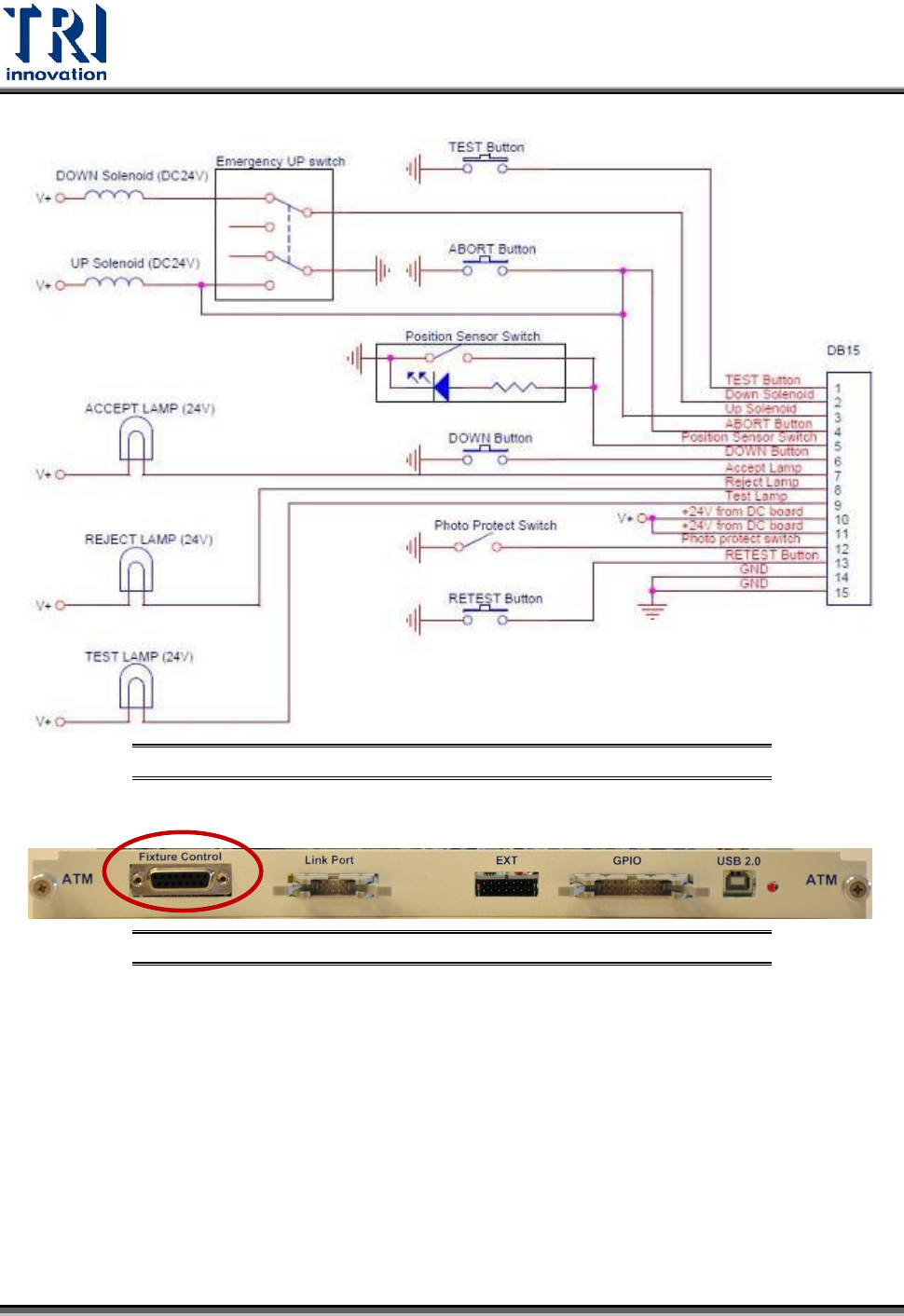
Test R esearch Inc. TR518 SII 使用手冊 --- 硬體 規格與架構 17 3.2.26 Press Unit 介面 Press Unit Inter face at ATM board 針位定義 : PIN Signal Name 1 TEST_Button 2 Down_Sol enoid 3 Up_Solenoi d 4 ABORT_Button 5 Position_Sen sor_Switch…
Test Research Inc.
16 TR518 SII 使用手冊---硬體規格與架構
3.2.23 DACs (數位-轉-類比的轉換器)
Resolution : 12 bits
Accuracy : +/- 1 LSB
3.2.24 ADCs (類比-轉-數位的轉換器)
Resolution: 14 bits
Conversion Time : 50nS
Accuracy : +/- 4 LSBs (max)
3.2.25 通用型 輸入/輸出 (GPIO)
TTL Input : Maximum 24V
Open collect output : Maximum 24V
Over Current Protection
- Build-in diagnostic hardware
- Auto Calibration
- USB 2.0 / PCIe interface with NetBook/Notebook/Desktop PC
Test Research Inc.
TR518 SII 使用手冊---硬體規格與架構 17
3.2.26 Press Unit 介面
Press Unit Interface at ATM board
針位定義:
PIN
Signal Name
1
TEST_Button
2
Down_Solenoid
3
Up_Solenoid
4
ABORT_Button
5
Position_Sensor_Switch
6
DOWN_Button
7
Accept_Lamp
8
Reject_Lamp
9
Test_Lamp
10
+24V
11
+24V
12
Photo Protect Switch
13
RESET_Button
14
GND
15
GND
Test Research Inc.
18 TR518 SII 使用手冊---硬體規格與架構
Figure 6: Analog Test Module (ATM) Board --- Press Unit
介面
Figure 7: Press Unit
在
ATM board
上的位置