2500_Users_Manual-.pdf - 第81页
Tasks and Kits Description EPROM task using the systen def emits. Process( es) 1 Z 3 r 3 r 3 r i x Z7 Data S C ) ( • ) ( ) Uord Uidth: I/O Offset: I/O Begin : I/O Block: Begin RAM: Begin Device: Device Block: MeMory Devi…
Device(s)
Data Source
Data File Translation Format
Process(es)
< More... > Handling/Labeling Parameters...
Tasks
and
Kits
Dev
ice(
s)
k
Z751ZX
PC
Disk
File
|u47b.
£93
Data
Source
( )
None
(
)
Host
Download
(♦)
PC
Disk
File
( )
Terninal/Host
( )
Master
Device
(
)
PrograMMer
Disk
Description
lEPROM
task
using
the
systen
defaults.
Process(
es)
12m
[][][]
Blank
Check
[XJ
[
J
[
J
rx]
r
]
r
i
[>□
rx]
[
i
rx:
rxi
[
i
Illegal
B
it
PrograM
Uerify
Label
PrograMMer
Type
Default
Handler
Type
Default,
Translation
Format
(83)
Intel
MCS-86
Edit
Task
"MEMORY
TASK"
Enter
text
;
Tab
for
next
iteM
<
Fl=Help
Data
Sumcheck
•
Serial
Vector
Test
—
The
2500
applies
test
vectors
to
the
device
inputs
in
parallel.
If
the
PLD
design
requires
certain
input
pins
to
be
applied
before
others,
the
JEDEC
standard
states
that
the
test
vectors
must
be
written
to
enforce
that
particular
order.
When
this
option
has
been
selected,
the
2500
applies
the
vector
inputs
starting
with
device
pin
1
and
continuing
in
numeric
order
to
the
last
input.
This
option
will
not
harm
the
device
and
should
be
used
as
a
troubleshooting
tool
when
a
large
number
of
devices
are
passing
fuse
verify
but
failing
test
vectors.
It
is
not
enabled
by
default.
•
DIP/LCC
vector
translation
—
In
some
instances
the
test
vectors
in
the
JEDEC
file
were
written
for
a
DIP
device
but
will
be
used
to
verify
a
PLCC
part.
When
this
translation
option
is
selected,
the
2500
automatically
translates
the
DIP
test
vectors
during
the
download
into
the
correct
format
to
test
the
PLCC/LCC
part.
This
optional
parameter,
when
selected,
will
check
the
sumcheck
at
the
end
of
the
file
transfer
with
the
sumcheck
entered
in
this
Task
field.
For
additional
information
on
this
parameter,
see
page
3-18.
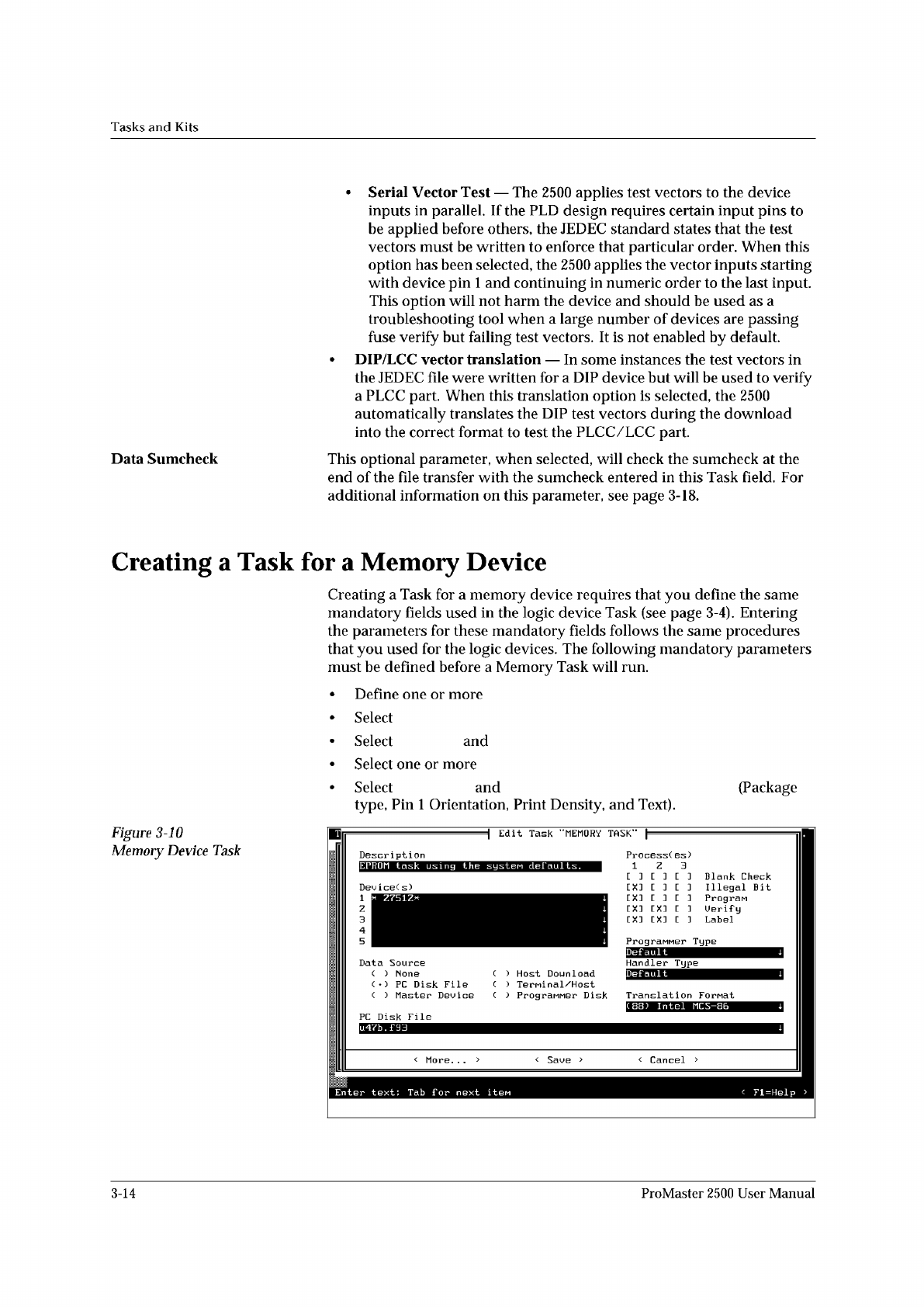
Creating
a
Task
for
a
Memory
Device
Creating
a
Task
for
a
memory
device
requires
that
you
define
the
same
mandatory
fields
used
in
the
logic
device
Task
(see
page
3-4).
Entering
the
parameters
for
these
mandatory
fields
follows
the
same
procedures
that
you
used
for
the
logic
devices.
The
following
mandatory
parameters
must
be
defined
before
a
Memory
Task
will
run.
•
Define
one
or
more
•
Select
•
Select
and
•
Select
one
or
more
•
Select
and
(Package
type,
Pin
1
Orientation,
Print
Density,
and
Text).
Figure
3-10
Memory
Device
Task
1
z
3
4
5
3-14
ProMaster
2500
User
Manual
Tasks
and
Kits
Description
EPROM
task
using
the
systen
def
emits.
Process(
es)
1
Z
3
r
3
r
3
r
i
x
Z7
Data
S
C
)
(
•
)
( )
Uord
Uidth:
I/O
Offset:
I/O
Begin
:
I/O
Block:
Begin
RAM:
Begin
Device:
Device
Block:
MeMory
Device
Parameters
卜
雷
FFFFFFFF
000000
000000
000000
000000
000000
Automatic
RAM
Fill
( )
None
( )
Default
( )
Specif
ic
[ ]
Odd/Euen
Byte
Swap
PC
Dis
u
47b.
<
OK
Cancel
>
Blank
Check
^=^=n
Bit
Edit
Task
"MEMORY
TASK"
Enter
deciMal
nunber
(
digits
0—9
)
;
Tab
f
or
next
it
巳
m
<
Fl=Help
>
<
MORE.
..
> <
Cancel
>
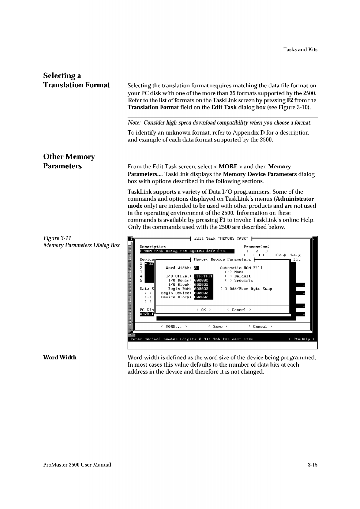
Selecting
a
Translation
Format
Other
Memory
Parameters
Figure
3-11
Memory
Parameters
Dialog
Box
Selecting
the
translation
format
requires
matching
the
data
file
format
on
your
PC
disk
with
one
of
the
more
than
35
formats
supported
by
the
2500.
Refer
to
the
list
of
formats
on
the
TaskLink
screen
by
pressing
F2
from
the
Translation
Format
field
on
the
Edit
Task
dialog
box
(see
Figure
3-10).
Note:
Consider
high-speed
download
compatibility
when
you
choose
a
format.
To
identify
an
unknown
format,
refer
to
Appendix
D
for
a
description
and
example
of
each
data
format
supported
by
the
2500.
From
the
Edit
Task
screen,
select
<
MORE
>
and
then
Memory
Parameters....
TaskLink
displays
the
Memory
Device
Parameters
dialog
box
with
options
described
in
the
following
sections.
TaskLink
supports
a
variety
of
Data
I/O
programmers.
Some
of
the
commands
and
options
displayed
on
TaskLink's
menus
(Administrator
mode
only)
are
intended
to
be
used
with
other
products
and
are
not
used
in
the
operating
environment
of
the
2500.
Information
on
these
commands
is
available
by
pressing
Fl
to
invoke
TaskLink's
online
Help.
Only
the
commands
used
with
the
2500
are
described
below.
Word
Width
Word
width
is
defined
as
the
word
size
of
the
device
being
programmed.
In
most
cases
this
value
defaults
to
the
number
of
data
bits
at
each
address
in
the
device
and
therefore
it
is
not
changed.
D
1
z
3
4
5
ProMaster
2500
User
Manual
3-15
Tasks
and
Kits
There
is
one
situation
when
the
word
width
value
would
be
changed.
This
occurs
if
you
are
trying
to
program
16-bit
RAM
data
into
two
8-bit
memory
devices.
Assume
that
the
2500
loads
a
file
intended
to
program
16-bit
data
into
two
8-bit
devices.
The
low
order
bytes
of
each
16-bit
word
are
saved
to
all
even
address
in
RAM
beginning
with
RAM
address
0
(zero).
The
high
order
bytes
for
each
word
would
be
stored
at
RAM
address
1
and
all
odd
address
locations.
If
the
default
parameters
are
not
changed,
the
2500
would
program
an
8-bit
device
(without
any
errors)
with
both
odd
and
even
bytes.
The
device
would
not
operate
in
a
16-bit
data
circuit.
To
program
all
low
order
bytes
into
one
8-bit
device
and
all
the
high
order
bytes
into
the
second
8-bit
device,
the
word
width
should
be
set
as
if
it
were
one
“virtual”
16-bit
device.
The
two
8-bit
devices
will
operate
in
their
target
circuit
application
“virtually”
as
if
they
were
a
single
16-bit
device.
To
program
a
virtual
16-bit
device
using
two
8-bit
parts,
perform
the
following
steps:
1.
Create
two
Tasks,
one
for
each
8-bit
device
that
downloads
the
same
16-bit
data
file.
In
the
first
Task,
Set
Word
Width
=
16
(see
Figure
3-11),
and
Set
Begin
RAM
=
0
(default).
2.
Create
a
second
Task
exactly
the
same
as
the
first
except:
Set
Begin
RAM
=
1.
3.
Load
the
first
Task.
4.
Program
the
number
of
devices
required.
The
combination
of
these
two
parameters
instructs
the
2500
to
program
the
device
from
all
even
RAM
addresses,
beginning
with
address
0.
This
creates
the
low
order
device
in
the
two-device
set.
5.
Load
the
second
Task.
6.
Program
the
number
of
devices
equal
to
the
number
programmed
by
the
first
Task.
The
2500
programs
the
second
device
from
all
odd
RAM
addresses,
beginning
with
RAM
address
1.
This
creates
the
high
order
device
in
the
two
device
set.
Setting
I/O
Offset
I/O
Offset
is
a
value
that
is
subtracted
from
each
file
address
during
a
data
file
download
from
the
PC
to
the
2500's
RAM.
During
a
data
file
upload
from
the
2500's
RAM
to
a
PC
file,
the
I/O
Offset
value
is
added
to
the
RAM
address
before
it
is
transmitted.
The
following
example
uses
a
file
download,
because
it
is
the
most
common
application.
File
Download:
File
address
number
-
I/O
offset
number
xxxx xxxx
+
Beginning
RAM
address
number
2500
RAM
address
=
YYYY
YYYY
3-16
ProMaster
2500
User
Manual