IPC J-STD-003B.pdf - 第17页
4.2 Tests with Established Accept/Reject Criteria 4.2.1 Test A – Edge Dip Test Tin/Lead Solder This test is for edge dip testing of surface conductors and attachment lands. 4.2.1.1 Apparatus 4.2.1.1.1 Solder Pot/Bath A s…

4 TEST PROCEDURES
4.1 Test Procedure Limitations
The test procedures of
this specification are applicable to most printed board con-
structions typical of the industry. It is recognized that thick
printed boards will not act the same as thin printed boards
due to their increased thermal mass, aspect ratio, number of
ground planes and weight of the solder column within the
hole. These factors greatly reduce the likelihood that all
holes will display completely wetted knees with top side
caps.
The test procedures of this specification shall be followed.
If determined by an agreement between the user and ven-
dor that changes are necessary due to the physical charac-
teristics of a test specimen and not the solderability of the
test specimen surface, a new procedure shall be docu-
mented and used only for the applicable test specimen.
Changes in test procedures and flux (see 3.2.2) shall take
into account the wetting time and flux issues per 6.6 and
6.7.
4.1.1 Application of Flux The test specimens are to be
dipped in the flux to the full depth to be soldered for 5-10
seconds. The flux shall be maintained at the prescribed
composition defined in 3.2.2. After withdrawal from the
flux, the test specimen shall be allowed to drain vertically
for a maximum of 60 seconds. Excess flux shall be
removed by blotting the surface to be tested with a piece of
absorbent, clean material. The solderability test shall then
be performed in not less than one minute, and not more
than five minutes, after blotting.
IPC J-STD-003B March 2007
6
Copyright Association Connecting Electronics Industries
Provided by IHS under license with IPC
Not for Resale
No reproduction or networking permitted without license from IHS
--`,,```,,,,````-`-`,,`,,`,`,,`---
//^:^^#^~^^"^~"^"^:$^~#:"#:$@:~^"$^:#*~^$^~:^#*^^:^^*\\
4.2 Tests with Established Accept/Reject Criteria
4.2.1 Test A – Edge Dip Test Tin/Lead Solder
This test
is for edge dip testing of surface conductors and attachment
lands.
4.2.1.1 Apparatus
4.2.1.1.1 Solder Pot/Bath
A solder vessel that meets the
requirements of 3.3.2 shall be used. The solder shall meet
the requirements of 3.2.1. Solder bath temperatures and
solder contamination control shall be in accordance with
3.5.1 and 3.5.2.
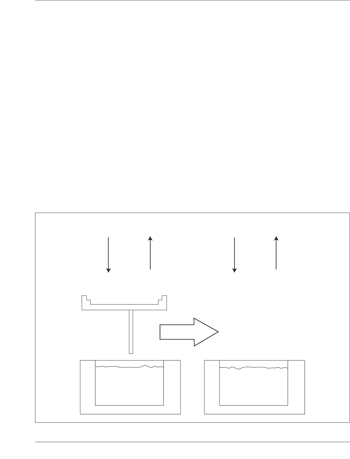
4.2.1.1.2 Dipping Device A dipping device as shown in
Figure 4-1 shall be used. A similar device may be used
providing: the rate of immersion, dwell time, and rate of
withdrawal are within the test limits; perpendicularity of
board and solder surface are maintained; wobble, vibration,
and other extraneous movements are eliminated.
4.2.1.2 Test Specimen The test specimen shall be a rep-
resentative portion of the board, or a full board, whichever
is smaller, not to exceed 50 x 50 mm [1.97 x 1.97 in], or a
test specimen that is representative of the common board
features. Figures 4-2 and 4-3 are suggested test specimen
styles. Test specimen preparation shall be in accordance
with 3.4.
Note: Relative to Figure 4-3, it is imperative that the met-
allization extends to the edge of the test specimen, in order
to guarantee a repeatable and accurate test. This is achieved
by imaging the test specimen larger in the multi-test speci-
men panel format than as it would otherwise have been
done as an individual test specimen. The singulation pro-
cess (removing the individual test specimens from the
multi-image panel) will have the scoring or routing path
pass through the oversize copper image, thus insuring that
the copper is fully present to the edge of the test specimen.
Due to the relative softness of the copper, the rough edge
may need to be ‘dressed’ using 600 grit sandpaper. An
alternate method to ensure that the copper is fully to the
edge of the test coupon is to preroute the test specimen and
edge plate. This latter alternative is generally more costly
and may not be available from all printed circuit board
fabricators.
4.2.1.3 Procedure Dross and burned/residual flux shall
be completely removed from the surface of the molten sol-
der immediately prior to dipping. After fluxing and drain-
ing per 4.1, the test specimen shall be immersed into the
molten solder edgewise to a depth of 25 ± 2 mm [0.984 ±
Flux
Initial Step
Process Flow
Insert
Specimen
Insert
Specimen
Withdraw
Specimen
Withdraw
Specimen
Station
Solder
Station
Final Step
IPC-003b-4-1
Figure 4-1 Edge Dip Solderability Test
March 2007 IPC J-STD-003B
7
Copyright Association Connecting Electronics Industries
Provided by IHS under license with IPC
Not for Resale
No reproduction or networking permitted without license from IHS
--`,,```,,,,````-`-`,,`,,`,`,,`---
//^:^^#^~^^"^~"^"^:$^~#:"#:$@:~^"$^:#*~^$^~:^#*^^:^^*\\
27.5 mm
[1.081 in]
2.0 mm
[0.0787 in]
22.5 mm
[0.8858 in]
7.5 mm [0.295 in]
2.5 mm [0.0984 in]
2.5 mm [0.0984 in]
Land Size 1.5 mm [0.0591 in]
40 Plated Through-Holes
0.8 ± 0.0125 mm [0.031 ± 0.0004921 in]
3.0 mm
[0.118 in]
2.5 mm
[0.0984 in]
9 Spaces @
S
Layer 1 Only
Appropriate
Specimen
Number
IPC-003b-4-2
Figure 4-2 Suggested Test Specimen for Plated-Through Holes
COMPONENT SIDE VIEW
Test Coupon size = 25 mm x 15 mm [0.984 in x 0.591 in]
SMD Pad Size = 3.18 mm x 4.52 mm [0.1250 in x 0.1780 in]
Pads are extended 0.51 mm [0.020 in] beyond the edge
Pad to pad pitch = 4.0 mm [0.157 in]
Mask clearance = 3.58 mm x 4.94 mm [0.1410 in x 0.1945 in]
Both sides
2.54 mm [0.1000 in]
0.94 mm [0.0370 in]
Pad Size (dia.) = 1.9 mm [0.0748 in]
Pad to pad pitch = 4.0 mm [0.157 in]
PTH size = 1.15 mm [0.0453 in] finished
Mask clearance = 2.31 mm [0.0909 in]
Both sides
IPC-003b-4-3
Figure 4-3 Suggested Test Specimen for Surface Mount Features
IPC J-STD-003B March 2007
8
Copyright Association Connecting Electronics Industries
Provided by IHS under license with IPC
Not for Resale
No reproduction or networking permitted without license from IHS
--`,,```,,,,````-`-`,,`,,`,`,,`---
//^:^^#^~^^"^~"^"^:$^~#:"#:$@:~^"$^:#*~^$^~:^#*^^:^^*\\